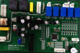
PCB design is a better art without the best. A PCB design with excellent performance often faces the challenge of the R&D cycle.
Statistics show that the design of a notebook usually takes only half a year from project approval to market launch. The research and development of a mobile phone, from project approval to market launch, takes only 3 months on average. As an important part of product development, PCB design time has gradually been compressed, compressed and then compressed.
In April 1985, a machine named T1100 pocketed the rise of the computer industry. Since then, the development cycle of computer motherboards has also accelerated significantly.
Way of working
Individual combat
3 people relay 3 shifts
Concurrent design
Design time
30 days
18 days
15 days
advantage
Single person responsible, no handover in the middle, low communication cost
Faster delivery, multi-person wisdom
Flexible delivery, easy to control, multiple people working at the same time, easy to communicate, and multiple people wise.
shortcoming
Long cycle, limited knowledge

PCB engineers are difficult to accept, the night shift efficiency is low, communication with surrounding resources is inconvenient, and the delivery efficiency is low due to 3 handovers
A certain team size is required, and personnel efficiency is slightly reduced.
Scope of application
Suitable for small companies or simple boards.
No need to communicate with surrounding resources, complex veneer, use with parallel design in special cases
Complex or more complex veneer, short design cycle. Widely used in large and medium EDA teams
Secondly, intervene in the product development process in advance to reduce subsequent rework. In the overall plan design stage, PCB engineers will intervene in research and development, focusing on the product system architecture design and demonstration; in the overall design stage, carry out the initial PCB design feasibility assessment; in the detailed design stage In the stage, the design of the principle scheme is synchronized, and the device selection, structural design, and thermal design are involved, so that when the R&D enters the PCB design process, the main work is simplified, and at the same time, it reduces the size of the device, insufficient drive capability, and infeasibility of the topology. And rework in the PCB design process caused by problems such as structural heat dissipation.
Again, the design concept of "one board success"
A senior consultant from IBM once pointed out the problems of a domestic R&D team: "There is no time to do things well at one time, but there is time to do things again and again." In the current market competition environment, they have experienced PCB design. Engineers, improve the design process, and use various tools and software to strive for success. It saves not only the cost of making a PCB, but also a whole-process research and development cycle. Win a window of market opportunity for the product. Both the PCB engineer himself and the product development supervisor must have the concept of "one board success" in PCB research and development.
Finally, module reuse, pay attention to technology precipitation
Many domestic well-known PCB companies attach great importance to the reuse of modules. While ensuring technology precipitation, they also effectively shorten the PCB design time.
In short, we must intervene in research and development in advance in the design concept, adopt parallel design, adopt the concept of one board success, reduce the number of research and development, plus advanced tools such as Cadence PSD, we do not need to work excessively overtime, let alone two shifts or even Three shifts can solve the PCB development cycle problem.