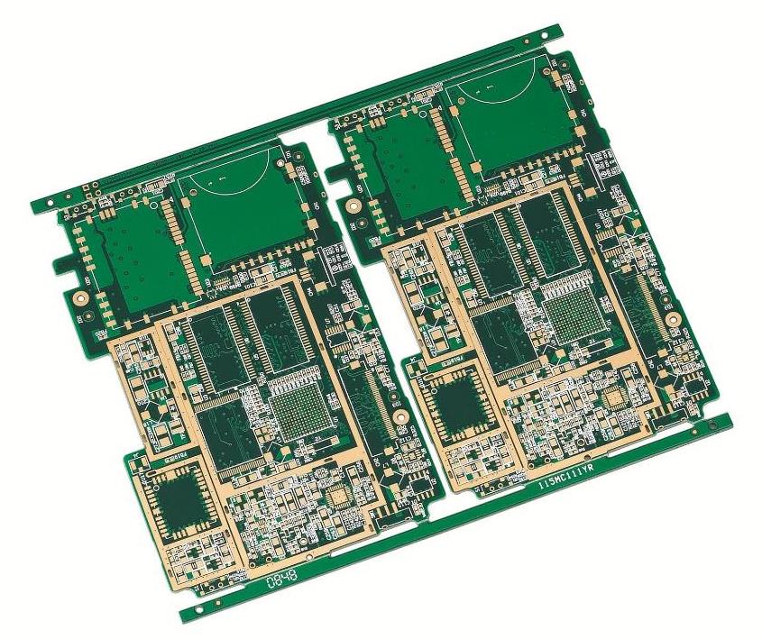
With the use of high-speed devices, there will be more and more high-speed DSP (digital signal processing) system designs, and processing signal problems in high-speed DSP application systems has become an important design issue. In this design, its characteristic is that the system data rate, clock rate and circuit density are constantly increasing, and the design of its PCB board shows completely different behavior characteristics from the low-speed design, that is, signal integrity problems and aggravated interference problems occur., Electromagnetic compatibility issues, etc.
These problems can cause or directly cause signal distortion, timing errors, incorrect data, address and control lines, system errors, and even system crashes. Failure to solve them will seriously affect system performance and bring immeasurable losses. The method to solve these problems mainly depends on the circuit design. Therefore, the design quality of the PCB board is very important. It is the only way to transform the optimal design concept into reality. The following discusses several issues that should be paid attention to in the reliability design of PCB boards in high-speed DSP systems.
1. Power supply design
High-speed DSP system PCB board design first needs to consider the power supply design problem. In power supply design, the following methods are usually used to solve signal integrity problems.
1. Consider the decoupling of power and ground
Regardless of whether the circuit board has a dedicated ground layer and power layer, a certain and reasonably distributed capacitor must be added between the power supply and the ground. In order to save space and reduce the number of through holes, it is recommended to use more chip capacitors. The chip capacitor can be placed on the back of the PCB board, that is, the soldering surface.

The chip capacitor is connected to the through hole with a wide wire and connected to the power supply and the ground through the through hole.
2. Wiring rules considering power distribution
separate analog and digital power layers
High-speed and high-precision analog components are very sensitive to digital signals. For example, the amplifier will amplify the switching noise to make it close to the pulse signal, so the analog and digital parts of the board, the power layer is generally required to be separated.
3. Isolate sensitive signals
Some sensitive signals (such as high-frequency clocks) are particularly sensitive to noise interference, and high-level isolation measures must be taken for them. The high-frequency clock (a clock above 20MHz, or a clock with a flip time of less than 5ns) must have a ground wire escort, the clock line width should be at least 10mil, and the escort ground wire width should be at least 20mil. The hole is in good contact with the ground, and every 5cm is punched to connect with the ground; a 22Ω~220Ω damping resistor must be connected in series on the clock sending side. The interference caused by the signal noise brought by these lines can be avoided.
2. Software and hardware anti-jamming design
Generally, high-speed DSP application system PCB boards are designed by users according to the specific requirements of the system. Due to limited design capabilities and laboratory conditions, if perfect and reliable anti-interference measures are not taken, once the working environment is not ideal, there is electromagnetic Interference will cause the DSP program flow to be disordered. When the DSP's normal working code cannot be restored, the program will run away or crash, and some components may even be damaged. Attention should be paid to taking corresponding anti-interference measures.
1. Hardware anti-interference design
The hardware anti-jamming efficiency is high. When the system complexity, cost, and volume are tolerable, the hardware anti-jamming design is preferred. Commonly used hardware anti-jamming technologies can be summarized as the following:
(1) Hardware filtering: RC filter can greatly attenuate all kinds of high-frequency interference signals. For example, the interference of "burr" can be suppressed.
(2) Reasonable grounding: Reasonable design of grounding system. For high-speed digital and analog circuit systems, it is important to have a low-impedance, large-area grounding layer. The ground layer can not only provide a low-impedance return path for high-frequency currents, but also make EMI and RFI smaller, and it also has a shielding effect on external interference. Separate the analog ground from the digital ground during PCB design.
(3) Shielding measures: AC power, high-frequency power, high-voltage equipment, and electric sparks generated by arcs will generate electromagnetic waves and become noise sources of electromagnetic interference. Metal shells can be used to surround the above-mentioned devices and ground them. This pair of shields The interference caused by electromagnetic induction is very effective.
2. Software anti-jamming design
Software anti-jamming has the advantage that hardware anti-jamming cannot replace. In the DSP application system, the anti-jamming ability of software should also be fully tapped to minimize the influence of interference. Several effective software anti-jamming methods are given below.
(1) Digital filtering: The noise of the analog input signal can be eliminated by digital filtering. Commonly used digital filtering techniques are: median filtering, arithmetic mean filtering and so on.
(2) Set trap: set up a section of boot program in the unused program area. When the program is disturbed and jump to this area, the boot program will forcibly guide the captured program to the specified address, and use a special program to correct the error program there. To process.
(3) Instruction redundancy: Insert two or three bytes of no-operation instruction NOP after the two-byte instruction and the three-byte instruction, which can prevent the program from being automatically brought into the right track when the DSP system is disturbed by the program running away.
Three, electromagnetic compatibility design
Electromagnetic compatibility refers to the ability of electronic equipment to work normally in a complex electromagnetic environment. The purpose of electromagnetic compatibility design is to enable electronic equipment to suppress all kinds of external interference, but also to reduce the electromagnetic interference of electronic equipment to other electronic equipment. In the actual PCB board, there is more or less electromagnetic interference phenomenon, that is, crosstalk between adjacent signals. The size of the crosstalk is related to the distributed capacitance and distributed inductance between the loops. To solve this kind of mutual electromagnetic interference between signals, the following measures can be taken:
1. Choose a reasonable wire width
The impact of the transient current on the printed lines is mainly caused by the inductance of the printed wires, and its inductance is proportional to the length of the printed wires and inversely proportional to the width. Therefore, the use of short and wide wires is beneficial to suppress interference. The signal wires of clock leads and bus drivers often have large transient currents, and their printed wires should be as short as possible. For discrete component circuits, the printed wire width is about 1.5mm to meet the requirements; for integrated circuits, the printed wire width is selected between 0.2mm to 1.0mm.
2. Adopt a grid-shaped wiring structure in a tic-tac-toe.
The specific method is to wire horizontally on one layer of the PCB board and wire vertically on the next layer.
Fourth, heat dissipation design
In order to facilitate heat dissipation, the printed board is best to be installed on its own, and the board spacing should be greater than 2cm. At the same time, pay attention to the layout rules of the components on the printed board. In the horizontal direction, the high-power devices are arranged as close to the edge of the printed board as possible to shorten the heat transfer path; in the vertical direction, the high-power devices are arranged as close as possible to the top of the printed board, thereby reducing its impact on the temperature of other components. Components that are more sensitive to temperature should be placed in areas with relatively low temperature as much as possible, and should not be placed directly above devices that generate large amounts of heat.
In the various designs of high-speed DSP application systems, how to transform a perfect design from theory to reality depends on high-quality PCB boards. The operating frequency of DSP circuits is getting higher and higher, the pins are getting denser, and the interference is increasing., How to improve the quality of the signal is very important. Therefore, whether the performance of the system is good or not is inseparable from the quality of the PCB board of the PCB designer.