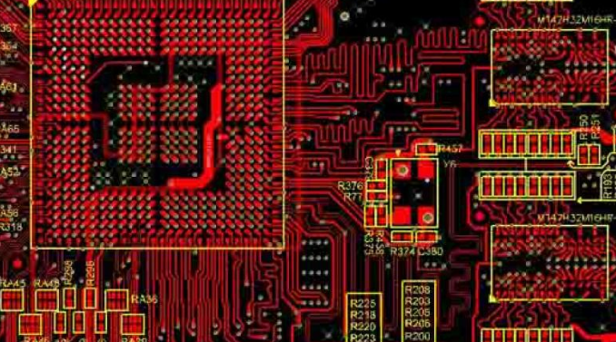
1. The rules of circuit layout of high-speed PCB circuit board manufacturers
PCB circuit layout can be understood as the way to lay the power signal in order to connect each component. In the initial planning process, wiring is an important process to complete product planning. Special attention is paid to the most detailed and limited process. For some experienced engineers, Is also a very brain-burning thing, so when we lay out the circuit board, we need to know the basic layout rules! 1. Direction: The input and output wires should be avoided as far as possible. The routing directions of adjacent layers are orthogonal to prevent different signal lines from running in the same direction on adjacent layers to reduce interference between layers. When PCB wiring is restricted by structure, it is difficult to prevent parallel wiring, especially in signal When the speed is higher, you should consider blocking each wiring layer with a ground plane and blocking each signal line with a ground wire.2. Length: When planning the PCB circuit board, the wiring length should be as short as possible to reduce the disturbance caused by the excessively long wiring.
3. Open loop inspection: In order to prevent the "antenna effect" of the wiring during PCB wiring, reduce unnecessary disturbing radiation, it is not allowed to show the wiring method with one end floating.4. Impedance matching check: The wiring width of the same network should be consistent.

Variations in line width will cause uneven line characteristic impedance. When the transmission speed is high, reflection will occur. This situation should be avoided in planning. Under certain conditions, such as the similar structure of the lead wire of the connector and the lead wire of the BGA package, the change of the line width may not be prevented, and the useful length of the center inconsistent part should be reduced as much as possible. 5. Chamfering: When PCB wiring, it is inevitable to bend the trace. When the trace has a right-angled corner, additional parasitic capacitance and parasitic inductance will occur at the corner. The corner of the trace should be prevented from being planned to be an acute or right-angled corner. Method, to avoid unnecessary radiation, and the process performance of acute angle and right angle method is also not good. It is required that the angle between all lines should be greater than or equal to 135°. In the situation where right-angled corners are really needed for routing, two ways to improve can be adopted: one is to turn 90° corners into two 45° corners; the other is to use rounded corners. The rounded corner method is the best. °The corner can be used at 10GHz frequency. Regarding the 45° corner wiring, the corner length should preferably satisfy L≥3W.6. Ground wire loop: The minimum rule of the loop, that is, the loop area formed by the signal wire and its loop should be as small as possible. The smaller the loop area, the less external radiation and the less interference from the outside world. 7, 3W rule: In order to reduce crosstalk between lines, the line distance should be large enough. When the line center distance is not less than 3 times the line width, 70% of the electric field can be maintained without interfering with each other, which is called the 3W rule. If you want to achieve 98% of the electric field without disturbing each other, you can use a distance of 10W. 8. Shielding protection: Corresponding to the rules of the ground loop, in practice, it is also to minimize the loop area of the signal, which is more common in some more important signals, such as clock signals and synchronization signals; for some particularly important and high-frequency signals, it should be Consider the use of copper shaft cable shielding structure planning, that is, to block the line up and down with ground wires, and also consider how to effectively combine the shielding ground with the practical ground plane.
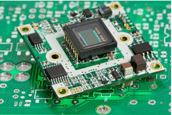
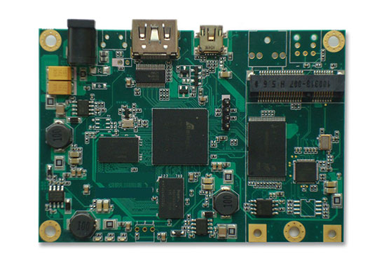
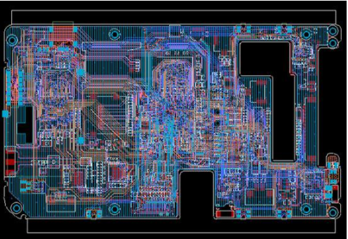
2. High-precision multilayer circuit board
PCB is the support of electronic components and the carrier of electrical connection of electronic components. The reason why PCB can be used more and more widely is that it has many unique advantages. Everyone knows that there are two Or multi-layer and two-layer PCB boards are laminated, which layers are included in the high-precision multi-layer circuit board, and how much do you know about the functions of each layer in the production process! Multi-layer PCB circuit boards include many types of working levels, Such as signal layer, protective layer, silk screen layer, internal layer, etc.
1. Signal layer: used to place components or wiring. Protel DXP usually contains 30 middle layers, namely Mid Layer1~Mid Layer30. The middle layer is used to arrange signal lines, and the top and bottom layers are used to place components or copper.2. Protective layer: used to ensure that the parts of the multilayer circuit board that do not need to be tinned are not tinned, so as to ensure the reliability of the operation of the multilayer circuit board. Among them, Top Paste and Bottom Paste are the top solder resist layer and the bottom solder resist layer, respectively. Top Solder and Bottom Solder are the solder paste protective layer and the bottom solder paste protective layer, respectively.3. Silk screen layer: used to print the serial number (position), production number, company logo, etc. of the components on the circuit board.4. Internal layer: used as a signal wiring layer, Protel DXP contains 16 internal layers.5. Other layers: drilling azimuth layer, forbidden wiring layer, drilling drawing layer, etc.