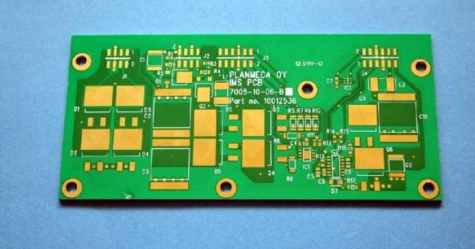
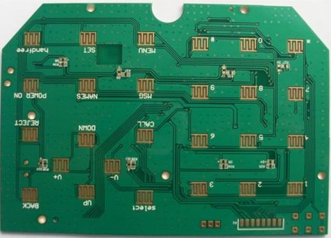
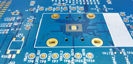
Creating a printed circuit board (PCB) that meets all design requirements can be a highly technical and time-consuming process-not to mention expensive. The task of the design engineer is to turn the concept into reality in the shortest possible time in order to accelerate the time to market through high-quality, reliable products.
EMI engineers should be able to theoretically analyze the generation of EMI, and mainly consider many practical EMI suppression methods and methods from the system design. Here we will analyze how to control EMI for high-speed PCB design.
1. Transmission line RLC parameters and EMI

For the PCB board, each trace on the PCB can be described by three basic distribution parameters, namely resistance, capacitance and inductance. In the control of EMI and impedance, inductance and capacitance play a great role.
Capacitors are components of electrical circuit systems that store electrical energy in the system. Between any two adjacent transmission lines, between two PCB conductive layers, and between the voltage layer and the surrounding ground plane can form a capacitor. Among all these capacitors, the capacitance between the transmission line and its return current has the largest value and the largest number, because any transmission line will flow back through some kind of conductive material around it. According to the capacitance formula: C=εs/(4kπd), the size of the capacitance formed between them is inversely proportional to the distance from the transmission line to the reference plane, and proportional to the diameter (cross-sectional area) of the transmission line. We all know that if the value of the capacitor is larger, the electric field energy stored between them will be more. In other words, the ratio of the system energy leaked to the outside will be less, so the EMI generated by the system will get a certain amount. Inhibition.
Inductance is a component in the circuit system that stores the energy of the surrounding magnetic field. The magnetic field is an induced field produced by the current flowing through the conductor. The value of the inductance indicates its ability to store the magnetic field around the conductor. If the magnetic field is weakened, the inductive reactance will become smaller. When the inductive reactance becomes larger, the magnetic field will increase, and the external magnetic energy radiation will also increase, that is, the EMI value. Bigger. Therefore, if the inductance of the system is smaller, then EMI can be suppressed. In the case of low-frequency PCB, if the conductor becomes shorter, thicker, and wider, the inductance of the conductor will become smaller. In the case of high-frequency PCB, the size of the magnetic field is proportional to the closed loop area formed by the wire and its return. Function, if the wire is close to its loop, since the return current and its own current are equal (in the best return state) and the directions are opposite, the magnetic fields generated by the two will cancel each other, reducing the inductance of the conductor, so the current on the conductor is maintained And its optimal return path can reduce EMI to a certain extent.