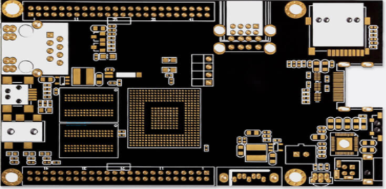
A common problem with switching power supplies is "unstable" switching waveforms. Sometimes, the waveform jitter is in the sound band, and the magnetic components will produce audio noise. If the problem lies in the layout of the printed circuit board, it may be difficult to find the cause. Therefore, the correct PCB layout at the initial stage of switching power supply design is very critical. The power supply designer must have a good understanding of the technical details and the functional requirements of the final product.
A good layout design can optimize power efficiency and reduce thermal stress; more importantly, it minimizes noise and the interaction between traces and components. To achieve these goals, the designer must understand the current conduction path and signal flow inside the switching power supply. To realize the correct layout design of non-isolated switching power supply, the following design elements must be kept in mind.
What are the tips for PCB layout design of non-isolated switching power supply
Layout planning?
The key is to plan the location of the power supply and the demand for board space in the early design and planning stages of the system. Sometimes designers ignore this advice and focus on the more "important" or "exciting" circuits on the large system board. Power management is regarded as an afterthought, and the power is placed on the extra space on the circuit board. This approach is very detrimental to high-efficiency and reliable power supply design.
For multilayer boards, a good method is to place a DC ground or DC input/output voltage layer between the high-current power component layer and the sensitive small signal trace layer. The ground layer or DC voltage layer provides an AC ground shielding small signal traces to prevent interference from high-noise power traces and power components. As a general rule, neither the ground plane nor the DC voltage plane of a multilayer PCB should be separated. If this separation is unavoidable, try to reduce the number and length of traces on these layers, and the layout of traces should be kept in the same direction as the high current to minimize the impact.
What are the tips for PCB layout design of non-isolated switching power supply
illustrate:

These structures sandwich the small signal layer between the high current power layer and the ground layer, thus increasing the capacitive noise coupled between the high current/voltage power layer and the analog small signal layer.
(b) and (d) are good structures for six-layer and four-layer PCB design respectively, which help to minimize the coupling noise between layers, and the ground layer is used to shield the small signal layer.
Be sure to place a ground layer next to the outer power level layer, and use thick copper foil for the external high-current power layer to minimize PCB conduction loss and thermal resistance.
The layout of the power stage?
The switching power supply circuit can be divided into two parts, the power stage circuit and the small signal control circuit. The power stage circuit contains components used to transmit large currents. Generally, these components should be placed first, and then small-signal control circuits should be placed at specific points in the layout. High-current traces should be short and wide to minimize PCB inductance, resistance, and voltage drop. For those traces with high di/dt pulse currents, this aspect is especially important.
1. Synchronous buck converter current path
What are the tips for PCB layout design of non-isolated switching power supply
The continuous current path and pulse current path in a synchronous buck converter. The solid line represents the continuous current path, and the dashed line represents the pulse (switch) current path. The pulse current path includes traces connected to the following components: input decoupling ceramic capacitor CHF, upper control FET QT and lower synchronous FET QB, and optional parallel Schottky diodes.
2. Parasitic inductance
What are the tips for PCB layout design of non-isolated switching power supply
Due to the parasitic inductance, the pulse current path not only radiates magnetic fields, but also generates large voltage ringing and spikes on PCB traces and MOSFETs. In order to minimize the PCB inductance, the pulse current loop (the so-called thermal loop) should have the smallest circumference when laying out, and its trace should be short and wide. The high frequency decoupling capacitor CHF should be 0.1μF~10μF, X5R or X7R dielectric ceramic capacitor, it has very low ESL (effective series inductance) and ESR (equivalent series resistance). Larger capacitor dielectrics (such as Y5V) may cause the capacitance value to drop significantly at different voltages and temperatures, so it is not the best material for CHF.