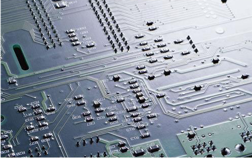
a. PCB component inspection
1, Confirm whether all device packages are consistent with the company's unified library, and whether the package library has been updated (use viewlog to check the running results). If they are inconsistent, be sure to Update Symbols
2, Mother board and daughter board, single board and back board, confirm that the signal corresponds, the position is corresponding, the connector direction and the silk screen identification are correct, and the daughter board has measures to prevent misplugging, the daughter board and the components on the mother board should not interfere
3. Whether the components are 100% placed
4. Turn on the place-bound of the TOP and BOTTOM layers of the device, and check whether the DRC caused by the overlap is allowed
5. Is the Mark point sufficient and necessary?
6, Heavier components should be placed close to the support point or edge of the PCB to reduce the warpage of the PCB
7. It is best to lock the devices related to the structure after they are deployed to prevent misoperation and movement.
8. Within 5mm of the crimp socket, no components whose height exceeds the height of the crimp socket on the front side, and no components or solder joints on the back side
9, Confirm whether the device layout meets the process requirements (focus on BGA, PLCC, patch sockets)

10. For the components of the metal shell, pay special attention not to collide with other components, and leave enough space.
11. The interface-related components should be placed as close to the interface as possible, and the backplane bus driver should be placed as close as possible to the backplane connector
12. Whether the CHIP device on the PCB wave soldering surface has been converted into a wave soldering package,
13, Whether there are more than 50 manual solder joints
21. For the axial insertion of higher components on the PCB, horizontal installation should be considered. Leave space for lying down. And consider the fixing method, such as the fixed pad of the crystal oscillator
14. For devices that require a heat sink, confirm that there is sufficient distance from other devices, and pay attention to the height of the main device within the range of the heat sink
b. Functional inspection
15, Whether the digital circuit and analog circuit components of the digital-analog hybrid board have been separated during the layout, and whether the signal flow is reasonable
16, A/D converter is placed across the analog-to-digital partition.
17, Is the clock device layout reasonable?
18. Is the layout of high-speed signal devices reasonable?
19. Whether the termination device has been placed reasonably (source matching series resistance should be placed at the driving end of the signal; middle matching series resistance should be placed in the middle position; terminal matching series resistance should be placed at the receiving end of the signal)
20. Is the number and location of the decoupling capacitors of the IC device reasonable?
21. The signal line uses planes of different levels as the reference plane. When crossing the plane division area, whether the connection capacitance between the reference planes is close to the signal routing area.
22. Whether the layout of the protection circuit is reasonable and whether it is conducive to division
23. Whether the fuse of the single board power supply is placed near the connector and there is no circuit component in front
24. Confirm that the strong signal and weak signal (the power difference is 30dB) are separately arranged in the circuit
33. Whether to place the devices that may affect the EMC experiment according to the design guide or refer to the successful experience. Such as: the reset circuit of the panel should be slightly close to the reset button
c. fever
25. Keep heat-sensitive components (including liquid medium capacitors, crystal oscillators) as far away as possible from high-power components, radiators and other heat sources
26. Whether the PCB layout meets the thermal design requirements and heat dissipation channels (implemented according to the process design documents)
d. Power
36. Is the IC power supply too far away from the IC?
37. Is the layout of the LDO and surrounding circuits reasonable?
38. Is the layout of the surrounding circuit such as the module power supply reasonable?
39. Is the overall layout of the power supply reasonable?
e. Rule setting
40. Are all simulation constraints added to the Constraint Manager correctly?
41. Whether the physical and electrical rules are set correctly (pay attention to the constraint settings of the power supply network and the ground network)
42, whether the spacing setting of Test Via and Test Pin is sufficient
43. Whether the thickness and plan of the PCB stackmeet the design and processing requirements
44. Have all the differential line impedances with characteristic impedance requirements been calculated and controlled by rules