When PCB circuit boards carry out SMT patch processing (SMT), there are usually three methods (based on the situation of opening the steel mesh): all manual, semi-automatic, and fully automatic. All manual is to brush the steel mesh, and the placement of electronic components is done manually. Semi-automatic means manually brushing the steel mesh and placing the electronic components on the automatic placement machine. Fully automatic means that both the brushing of steel mesh and the placement of electronic components are fully automated by machines and equipment. It is easy to understand for all manual workers. After all, people are alive, the smartest, and they can find ways to deal with emergencies. But the machinery and equipment are different, how does it know where to put this electronic component on the PCB? And it exactly corresponds to the pad, and the chip orientation can't be wrong. In the "PADS output BOM table and bit number map", everyone mentioned how to output the component coordinates, which will contain the position and orientation information of each component in the PCB.
The automatic placement machine performs positioning based on these data, but this requires an anchor point, and the Mark point exists as this anchor point. The smt placement machine will recognize this Mark point as an anchor point, and then identify the position and orientation of the electronic component based on the coordinate and orientation information.

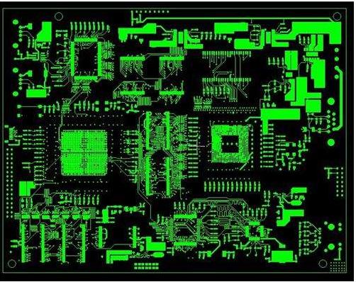
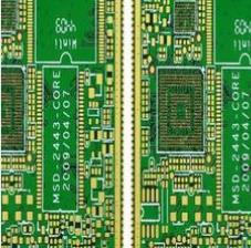
Usually the Mark points are placed on the diagonal of the single chip, and they appear in pairs, and the rectangle drawn on the diagonal should preferably include all the electronic components on the single chip. Naturally, it can also be done on the side of the craft, and it also needs to be placed diagonally and appear in pairs.
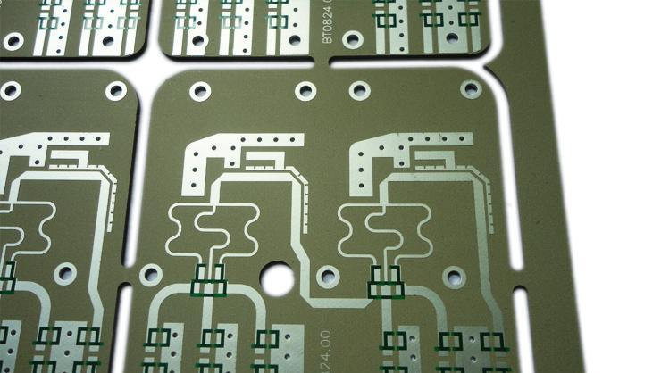
So what's the matter with the craft side? Similarly, if it is all manual, the craft edge may not be needed, because adding the craft edge requires more plates. However, in order to be able to use the smt placement machine, it is necessary to add a process edge, so that the smt placement machine can use the fixture to clamp the PCB. Naturally, if a single PCB circuit board is relatively large, and there are no electronic components 5mm away from the edge of the board, the process edge is not needed, and the clamp can directly clamp the board. In addition to adding Mark points on the process side, positioning holes need to be added. This is mainly used for testing.
After understanding the usefulness of the craft edge and the Mark point, let's take a look at the requirements of the two and how to add them.
1. Process side
The width is not less than 5mm, and the length is as long as the board. It can be used in jigsaw and single chip, and it can be marked with Mark points and positioning holes. The positioning hole is a through hole with a diameter of about 3mm.
The manufacturing method of the craft edge is similar to the puzzle. Use 2D lines to draw the same length as the PCB and 5mm width on all layers, and connect with the original PCB. The connection method can be V-cut, stamp hole or connecting strip., According to actual needs. The specific operation process can be seen in the video. The finished craft side.
2. Mark point
The Mark point has two parts, one is the mark in the middle with a diameter of 1mm; the other is a circular open area around the dot, the center of the circle coincides with the center of the mark in the middle, and the diameter is 3mm.
Mark point design method: enter the package editor and place a circular patch pad with a diameter of 1mm on the top layer.
Place a copper foil hollow area with a diameter of 3mm on the top layer:
Place a copper foil with a diameter of 3mm on the top solder mask
Just save it. When in use, directly enter the ECO mode and add Mark points to encapsulate. There can be no traces and 2D lines in the open area of the Mark points.
Design the PCB with process edges, Mark points and positioning holes.
The above is the function and production method of the process edge and Mark point. The specific details need to be modified according to the requirements of the PCB manufacturer.