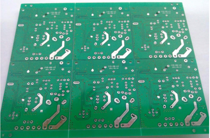
PCB engineering design should try to avoid structural asymmetry, material asymmetry, and graphic asymmetry design to reduce the occurrence of deformation. At the same time, it was found in the research process that the core board directly laminated structure is easier to deform than the copper foil laminated structure. The test results of a kind of structural panel.
There is a clear difference in the defect rate of the two structures with unqualified deformation. It can be understood that the core plate laminated structure is composed of three core plates, and the expansion and contraction and stress changes between different core plates are more complicated and difficult to eliminate. In engineering design, the frame form of the jigsaw panel also has a greater impact on the deformation. Generally, PCB factories will have a continuous large copper frame and a non-continuous copper dot or copper block frame, and there are also different differences.
Comparison test results of two kinds of frame design panels. The reason why the deformation of the two frame forms is different is that the continuous copper frame has high strength and greater rigidity during the pressing and splicing process, so that the residual stress in the board is not easy to release. It is concentrated on the release after the shape is processed. Lead to more serious deformation. The discontinuous copper dot frame gradually releases the stress during the pressing and subsequent processing, and the veneer deforms less after the shape. The above are some possible influencing factors involved in the engineering design, if they can be used flexibly in the design. It can reduce the influence of deformation caused by the design.

Compression Research
The impact of pressing on PCB deformation is very important. Reasonable parameter settings, press selection and stacking methods can effectively reduce stress. For general panels with symmetrical structures, it is generally necessary to pay attention to symmetrical stacking during pressing, and symmetrical placement of auxiliary tools such as tool panels and cushioning materials. At the same time, choosing the hot and cold integrated press to press is also obviously helpful to reduce the thermal stress. The reason is that the cold and hot split press transfers the plate to the cold press at high temperature (above GT temperature), and the material loses pressure above the Tg point. Rapid cooling will lead to rapid release of thermal stress and deformation, and the integrated cold and hot press can cool down the final stage of hot pressing and avoid the plate from losing pressure at high temperatures.
At the same time, for the special needs of customers, it is inevitable that there will be some plates with asymmetric materials or structures. At this time, the deformation caused by the different CTEs analyzed in the previous article will be very obvious. For this problem, we can try to use asymmetric The principle is to use the asymmetrical placement of the buffer material to achieve different heating speeds on both sides of the PCB, which affects the expansion and contraction of different CTE core cypresses during the heating and cooling stages to solve the problem of inconsistent deformation. Table 4 is the test result on a certain structural asymmetric plate of our company. Through the asymmetric stacking method, and adding a post-curing process after pressing, and leveling before shipment, this board finally meets the customer's 2.0mm requirements.
Other production processes
In the PCB production process, in addition to pressing, there are several high-temperature treatment processes for solder mask, characterization and hot air leveling. Among them, the highest temperature of the solder mask and the baking board after the character is 150 degree Celsius. As mentioned above, this temperature is in the ordinary Tg material. Above the Tg point, the material is in a highly elastic state and is easily deformed under external force. Therefore, avoid stacking the plates to prevent the lower plate from being bent when drying the plates. At the same time, ensure that the plate direction is parallel to the blowing direction when the plates are dried. In the hot air leveling process, it is necessary to ensure that the plate is placed in the tin furnace for cooling for more than 30 seconds to avoid the sudden cold deformation caused by the cold water washing of the post-treatment at high temperature.
In addition to the production process, the storage of PCB boards at each station also has a certain impact on the deformation. In some manufacturers, due to the large number of products to be produced and the small space, multiple boards are stacked together for storage, which will also cause the board The parts are deformed by external force, and because the PCB board also has a certain degree of plasticity, these deformations will not be 100% restored in the subsequent leveling process.
Leveling before shipment
Most PCB manufacturers will have a leveling process before shipment. This is because the deformation of the board caused by heat or mechanical force will inevitably occur during the processing. It can be leveled by mechanical leveling or thermal baking before shipment. Be effectively improved. Affected by the heat resistance of the solder mask and the surface coating layer, the general baking temperature is below 140 degree Celsius~150 degree Celsius, which just exceeds the Tg temperature of ordinary materials. This has great benefits for the leveling of ordinary boards, but for high Tg materials The leveling effect is not so obvious, so the temperature of the baking sheet can be appropriately increased on the high Tg boards with serious board warpage, but the quality of the ink and coating layer is mainly required. At the same time, the method of pressing weight during baking and increasing the cooling time with the furnace also has a certain effect on the deformation. The test results of the effect of different weight and furnace cooling time on the leveling of the plate can be seen from the increase in the weight and the extension of the furnace. The cold time has a significant effect on the leveling of deformation.