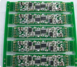
1. The difference between PCB laser cutting machine and metal laser cutting machine
PCB laser cutting machine and metal laser cutting machine are completely different products, so Baineng.com has sorted out the difference between PCB laser cutting machine and metal laser cutting machine to help you distinguish between the two products and accurately find the product that suits you. .
First of all, the laser light sources used by the two equipment are different. PCB laser cutting machines usually use ultraviolet lasers or green lasers; while metal laser cutting machines usually use fiber lasers or CO2 lasers; the working properties of the two equipment are relatively large. The difference, there is also a big difference in the power used. The power used by the PCB laser cutting machine generally does not exceed 30W (ultraviolet laser), while the metal laser cutting machine can reach more than 10KW (fiber laser) according to the thickness of the material.
Another part that needs to be distinguished is that in the PCB industry, some aluminum substrates or ceramic substrates use pulsed fiber lasers; and some manufacturers also use low-power CO2 lasers to process PCB circuit boards, usually lasers below 100W .

Secondly, the PCB laser cutting machine uses an ultraviolet laser, which is compatible with cutting ultra-thin metal materials below 0.2mm; while high-power optical fiber or CO2 cannot cut ultra-thin metal materials, which are prone to burrs, blackening, and deformation.
Second, the difference in cutting properties. PCB laser cutting machine adopts galvanometer scanning method, through multiple scanning back and forth, layer by layer is removed to form cutting; while metal laser cutting machine adopts collimating focusing system with coaxial auxiliary gas, which penetrates the material at one time Cutting.
Third, structural differences. Metal laser cutting machines usually use large gantry type machine tools with servo motors; while PCB laser cutting machines use marble stable platforms, linear motors, and standard CCD camera vision, relative position cutting accuracy, cutting size accuracy, The positioning accuracy is better than that of the metal laser cutting machine, and the two are different types of products.
Two, PCB design electrostatic analysis
In the design of the PCB board, the anti-ESD design of the PCB can be realized through layering, appropriate layout and installation. By adjusting the PCB layout and wiring, it is possible to prevent ESD well. Use multi-layer PCBs as much as possible. Compared with double-sided PCBs, the ground plane and power plane, as well as the closely arranged signal line-ground line spacing can reduce the common mode impedance. And inductive coupling, making it reach 1/10 to 1/100 of the double-sided PCB. There are components on the top and bottom surfaces, and there are very short connecting lines.
Static electricity from the human body, the environment, and even electronic equipment can cause various damages to precision semiconductor chips, such as penetrating the thin insulating layer inside the components; destroying the gates of MOSFET and CMOS components; and the triggers in CMOS devices are locked. ; Short-circuit reverse-biased PN junction; short-circuit forward-biased PN junction; melt the soldering wire or aluminum wire inside the active device. In order to eliminate electrostatic discharge (ESD) interference and damage to electronic equipment, a variety of technical measures need to be taken to prevent it.
In the design of the PCB board, the anti-ESD design of the PCB can be realized through layering, appropriate layout and installation. In the design process, the vast majority of design modifications can be limited to the addition or reduction of components through prediction. By adjusting the PCB layout and routing, ESD can be well prevented. The following are some common precautions.
Use multi-layer PCBs as much as possible. Compared with double-sided PCBs, the ground plane and power plane, as well as the tightly arranged signal line-ground spacing can reduce the common mode impedance and inductive coupling, making it 1/of the double-sided PCB. 10 to 1/100. Try to put each signal layer close to a power layer or ground layer. For high-density PCBs with components on the top and bottom surfaces, short connection lines, and many fills, you can consider using inner layer lines.
For double-sided PCBs, tightly interwoven power and ground grids are used. The power line is close to the ground line, and as many connections as possible between the vertical and horizontal lines or the filled area. The grid size on one side is less than or equal to 60mm. If possible, the grid size should be less than 13mm. Make sure that each circuit is as compact as possible.