Beginners compare the above basic principles one by one while wiring while drawing on the PCB board, and then use this rule to check again after the wiring is completed. Over time, there will be results. The ancients said: Foot, the ice is very hard. In the world, there are few geniuses after all, and only perseverance can achieve results. The word "gradual" almost implies the development and maturity of everything...
In addition, don't forget to add filtering and coupling capacitors between the power supply and ground of the integrated block to eliminate interference.
In addition, explain a misunderstanding of a PCB layout: some friends who only want to be quick, some friends who don’t want to really work hard on technology, some delusional friends always think that they can do PCB after learning some board-making software such as Protel/DXP., You can decorate the facade. And I said: Brother, don't be so naive. Technology, there is no shortcut! Maybe you are smarter, but you have to go through enough learning and practice. Otherwise, what you do is nothing but "good-looking"! Pragmatism is your duty to behave, and it is the minimum criterion for engineering.
Look at a board: Don't laugh at others with a few more jumpers!
Look at a board: Don't laugh at other people's hesitations and troubles!
If you laugh, first it means that you are not a good person, secondly it means that you are very superficial, and again it means that your skills are very poor...
Being a good person is like being a person, you can see your skill in every inch, and the subtlety reveals the spirit! Don't show off for publicity, just seek truth from the ground!

[Rule] 1: The schematic diagram is based on the principle of convenient wiring and troubleshooting, reasonable use of the bus, and the use of real pin distribution.
[Rule] 2: Before generating the PCB, the packages of all unfamiliar devices should be made by hand, and the triode package should be made in advance.
[Rule] 3: Manual sketching should be carried out before wiring, and general layout should be carried out under the principle of performance first.
[Rule] 4: The wiring should not be parallel to the axis of the component, carefully set the ground wire, and use full or grid copper plating appropriately.
[Rule] 5: The ground wire in the digital circuit should be networked, the signal clock wire should use snake walking wire reasonably, and the pad should be appropriate.
[Rule] 6: Manual wiring should be based on the network or component wiring, and then the docking and arrangement between the blocks.
[Rule] 7: When making emergency changes to the layout, you must be calm. Generally, you only need to change individual components or one or two networks.
[Rule] 8: When making PCB, leave at least five solder holes, four corners and the center, in the blank space for aligning holes.
[Rule] 9: It is best to brush the tin before soldering. The components are first placed on the board and fixed with tape before soldering.
[Rule] 10: The ADC circuit trace should be separated from the traces of other digital circuits or signal lines (especially clocks), and parallel and crossing are strictly prohibited.
[Rule] 11: The oscillating crystal should be as short as possible and surrounded by a ground wire, but be careful not to increase the load capacitance due to the small spacing.
[Rule] 12: Single and double panels must have at least 50% metal layers, and multilayer boards must have at least four metal layers to prevent local overheating and fire.
[Rule] 13: The signal wires should be as thick and short as possible, and ground wires should be added between signal wires and input and output wires, and ground wires should be clamped between each module.
[Rule] 14: When the device pin is in contact with the ground wire, it is better not to use a large area of copper, but to use a grid, and the whole board is also to use a grid to prevent peeling.
[Rule] 15: If there is a large area of copper on the PCB, several small openings should be made on the ground, but the hole should not be larger than 3.5mm, which is equivalent to a grid.
[Rule] 16: When using jumpers to avoid excessively long wiring, the jumpers should not be placed under large devices such as IC integrated blocks to facilitate plugging and unplugging.
[Rule] 17: The heat dissipation and ventilation of the device should be fully considered when layout and wiring, the heat source should be close to the edge of the board, and the distance between the test points should be designed.
[Rule] 18: In the multi-layer anti-electromagnetic interference design, the 20H rule and the 3W rule should be applied to overcome the boundary radiation coupling and logic current magnetic flux interference.
[Rule] 19: It is best not to have dual signal lines in the same direction of current, and to control the minimum parallel length, such as JOG routing or sine and cosine routing.
[Rule] 20: The interference caused by the change of the upper and lower edges of the signal in the low-frequency line is much greater than the interference caused by the frequency, so we must pay attention to the crosstalk problem.
[Rule] 21: The high-speed signal line should be added with appropriate termination matching, and it is best to keep its impedance unchanged during transmission, and widen the line width as much as possible.
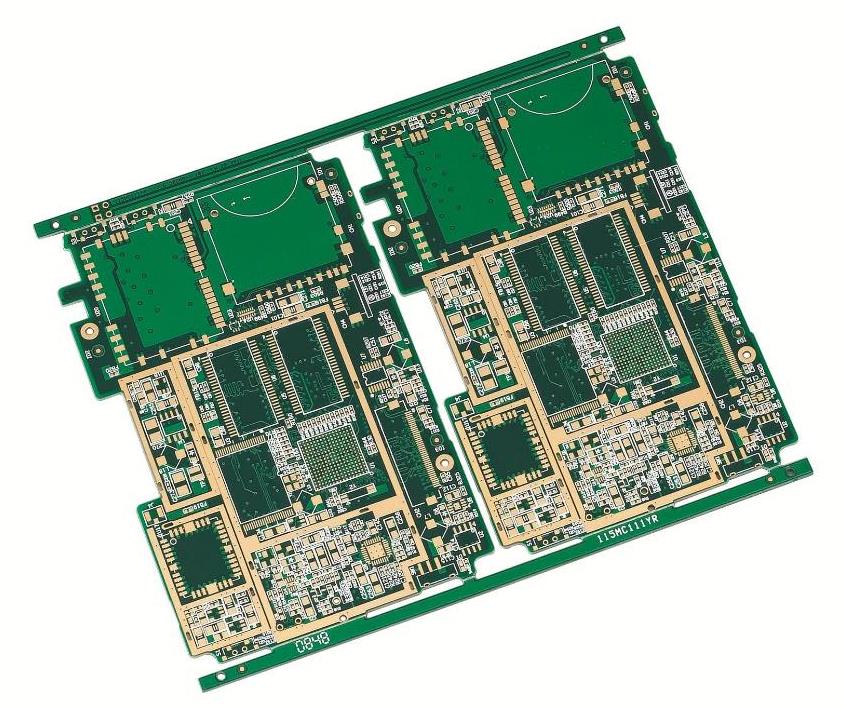
[Rule] 22: Don't think that PCB manufacturing is very simple, it only shows that your level needs to be improved. With the increasing density of modern integrated devices, the quality of the PCB layout directly affects the performance of the product, and even the key to the success or failure of the design. As an electronics expert in Japan said: There may be countless arrangements of ten kinds of devices. But if there is a little error, its performance may be a hundred times apart! The importance and technicality of PCB layout can be seen. I encountered some problems when making the board today, which caused the PCB I drew to not show any competitiveness!
When making holes for the board, because originally only single-sided boards were used and the layout method with one side blank was rarely used, some unexpected situations occurred when making double-sided boards with blank edges. Almost all the previous work was abandoned and the spirits were lethargic.
The lesson is now summarized as follows: when exporting data files of PCB solder holes and vias in EXPORT, the layout printed by the CNC machine tool is reversed from the layout displayed on the computer, or mirrored. That is: the actual board is the layout after turning 180 degrees to the right with the edge line on the right as the reference line in the circuit diagram. Pay special attention when there are blanks! Otherwise, the board will be useless!
When making a single panel, you can use three-point or five-point insertion and positioning method to align the holes of the board, or you can transfer the ink paper to the copper clad laminate first, and then use 0, 0 points or add a diagonal line. The method allows the CNC machine tool to automatically position and punch holes on it. However, since the naked eye points to the reference coordinate point, a slight error may cause all the holes to be misaligned. In this regard, be careful and patient!