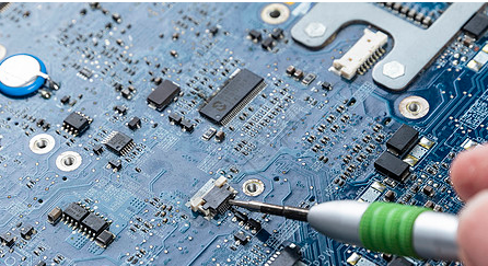
Mobile phone circuit board design skills
Mobile phone circuit board design to improve audio performance should:
Carefully consider the underlying planning. The ideal bottom plan should divide different types of circuits into different areas.
Use differential signals whenever possible. Audio devices with differential inputs can suppress noise. It is generally not possible to add a ground wire in the middle of the differential signal. Because the most important point of the application principle of differential signals is to use the benefits of mutual coupling between differential signals, such as magnetic flux elimination and noise immunity. If you add a ground wire in the middle, it will destroy the coupling effect.
There are two points to pay attention to in the layout of the differential pair. One is that the length of the two wires should be as long as possible, and the other is that the distance between the two wires (the distance is determined by the differential impedance) must be kept constant, that is, to keep parallel. There are two parallel ways, one is that the two wires run on the same side-by-side, and the other is that the two wires run on two adjacent layers above and below (over-under). Generally, the former has more side-by-side implementations.

Isolate the ground current to avoid the digital current from increasing the noise of the analog circuit. Basically, it is right to divide and isolate the analog/digital ground. It should be noted that the signal trace should not cross the divided place as much as possible, and the return current path of the power supply and signal should not change too much. The requirement that the digital-analog signal traces cannot cross is because the return current path of the digital signal with a faster speed will flow back to the source of the digital signal along the ground near the bottom of the trace as much as possible. If the digital-analog signal traces cross, the current will be returned. The generated noise will appear in the analog circuit area.
The analog circuit uses star grounding. The current consumption of audio power amplifiers is generally very large, which may have an adverse effect on their own grounding or other reference grounds.
Turn all unused areas on the circuit board into a ground plane. Realize grounding coverage near the signal traces to shunt the excess high-frequency energy in the signal lines to the ground through capacitive coupling.
Ultraviolet laser processing applications in the PCB industry
For laser cutting or drilling in the circuit board industry, only a few watts or more than ten watts of UV laser are required, and no kilowatt-level laser power is required. In consumer electronics, automotive industry or robot manufacturing technology, flexible circuit boards are Use becomes increasingly important. Because the UV laser processing system has flexible processing methods, high-precision processing effects and flexible and controllable processing, it has become the first choice for laser drilling and cutting of flexible circuit boards and thin PCBs.
Nowadays, the long-life laser source configured in the laser system is basically close to being maintenance-free. In the production process, the laser level is level 1, and no other protective devices are required for safety. The LPKF laser system is equipped with a dust collection device, which will not cause the emission of harmful substances. Coupled with its intuitive and easy-to-operate software control, laser technology is replacing traditional mechanical processes, saving the cost of special tools.
CO2 laser or UV laser?
For example, when PCB splitting or cutting, you can choose a CO2 laser system with a wavelength of about 10.6μm. The processing cost is relatively low, and the laser power provided can reach several kilowatts. But it will generate a lot of heat energy during the cutting process, which will cause severe carbonization of the edges.
The wavelength of the UV laser is 355 nm. Laser beams of this wavelength are very easy to focus optically. The spot diameter of a UV laser with a laser power of less than 20 watts is only 20μm after focusing-and the energy density it generates is even comparable to that of the sun's surface.
Advantages of UV laser processing
UV laser is especially suitable for cutting and marking hard boards, rigid-flex boards, flexible boards and their accessories. So what are the advantages of this laser process?
In the fields of circuit board sub-boarding in the SMT industry and micro-drilling in the PCB industry, the UV laser cutting system shows great technical advantages. Depending on the thickness of the circuit board material, the laser cuts one or more times along the required contour. The thinner the material, the faster the cutting speed. If the accumulated laser pulse is lower than the laser pulse required to penetrate the material, only scratches will appear on the surface of the material; therefore, two-dimensional code or barcode marking can be performed on the material for information tracking in subsequent processes.