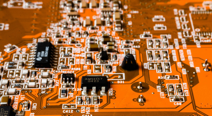
In SMT chip processing, reasonable planning and design of PCB circuit boards is a key step to ensure the quality of chip processing products. The main basic workflows are as follows:
SMT
1. PCB circuit board planning. It is mainly to plan the physical size of the PCB circuit board, the packaging form of the component, the component mounting method, and the layer structure (that is, the choice of single-layer board, double-layer board and multi-layer board).
2. Setting of working parameters. Mainly refers to the working environment parameter setting and the working layer parameter setting. Setting the PCB environmental parameters correctly and reasonably can bring great convenience to the design of the circuit board and improve work efficiency.
3. PCB component layout and adjustment. This is a relatively important task in PCB design, which directly affects the subsequent wiring and division of the internal electrical layer, so it needs to be treated carefully. After the current work is ready, the netlist can be imported into the PCB, or the netlist can be imported directly by updating the PCB in the schematic diagram.

You can use the Proteldxp software with its own automatic layout function, but the effect of the automatic layout function is often not ideal, and manual layout should generally be used, especially for complex circuits and components with special requirements.
4. PCB wiring rules setting. Mainly to set various specifications of circuit wiring, wire width, parallel line spacing, safety spacing between wires and pads, and via size, etc., no matter what wiring method is adopted, wiring rules are an indispensable step, good The wiring rules can ensure the safety of the circuit board wiring, and meet the requirements of the production process, saving costs.
5. PCB wiring and adjustment. The system provides automatic wiring, but it often fails to meet the designer's requirements. In actual applications, designers often rely on manual wiring, or partial automatic wiring combined with manual interactive wiring to complete the wiring work. Special attention should be paid to the characteristics of layout and wiring and PCB circuit boards with internal electrical layers. Although layout and wiring are in order, the layout of the circuit board is often adjusted according to the needs of wiring and internal electrical layer division in the design project, or According to the layout adjustment wiring, between them is a process of mutual consideration and mutual adjustment.
In addition, there are other auxiliary operations, such as copper coating and teardrop filling, as well as document processing work such as report output and save printing. These files can be used to check and modify PCB circuit boards, and can also be used as a list of purchased components. Only by doing these details can we better guarantee the product quality, and we can deal with and solve problems in time if we encounter problems.
The above is an introduction to the main work flow of PCB planning and design for SMT patch processing