Orifice plate design in PCB processing
The expansion and contraction of film and material during PCB production, the expansion and contraction of different materials during pressing, the position accuracy of pattern transfer and drilling, etc. will bring about inaccurate alignment between the patterns of each layer. In order to ensure the good interconnection of the patterns of each layer, the width of the pad ring must consider the requirements of the pattern alignment tolerance between the layers, the effective insulation gap and the reliability. Reflected in the design is to control the pad ring width.
(1) The metalized hole pad should be greater than or equal to 5mil.
(2) The width of the insulation ring is generally 10mil.
(3) The width of the anti-pad ring on the outer layer of the metallized hole should be greater than or equal to 6mil, which is mainly proposed in consideration of the needs of solder mask.
(4) The width of the anti-pad ring in the inner layer of the metallized hole should be greater than or equal to 8mil, which mainly considers the requirements of the insulation gap.
(5) The anti-pad ring width of non-metallized holes is generally designed as 12mil.

Solder mask design in PCB processing
The minimum solder mask gap, minimum solder mask bridge width, and minimum N cover expansion size depend on the solder mask pattern transfer method, surface treatment process and copper thickness. Therefore, if you need a more precise solder mask design, you need to know about the PCB board factory.
(1) Under the condition of 1OZ copper thickness, the solder mask gap is greater than or equal to 0.08mm (3mil).
(2) Under the condition of 1OZ copper thickness, the width of the solder mask bridge is greater than or equal to 0.10mm (4mil). Since the lm-Sn solution has an attacking effect on some solder resists, the width of the solder mask bridge needs to be increased moderately when using the surface treatment of the lm-Sn, and the minimum is generally 0.125mm (5mil).
(3) Under the condition of 1OZ copper thickness, the minimum expansion size of the conductor Tm cover is greater than or equal to 0.08mm (3mil).
The solder mask design of the via hole is an important part of the PCBA process manufacturability design. Whether to plug holes depends on the process path and the layout of the vias.
(1) There are three main methods for solder mask of via holes: plug hole (including half plug and full plug), open small window and open full window.
(2) Solder mask design of via holes under BGA
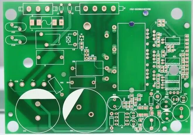
PCB schematic steps
1. Record PCB related details
Prepare a PCB and record the model, parameters, and positions of all components on the paper. You need to pay attention to the direction of the diode, the tertiary tube, and the direction of the IC gap. Then use a digital camera or mobile phone to take two photos of the location of the components.
2. Scanned image
Remove all the components on the PCB board and remove the tin in the PAD hole. Clean the PCB with alcohol and put it into the scanner. When the scanner scans, you need to raise the scanned pixels slightly to get a clearer image.
Then lightly sand the top and bottom layers with water gauze paper until the copper film is shiny, put them horizontally and vertically into the scanner, start ps, and scan the two layers separately in color.
3. Adjust and correct the image
Adjust the contrast and brightness of the canvas to make the part with copper film and the part without copper film have a strong contrast, then turn the second image into black and white, and check whether the lines are clear. If not, repeat this step. If it is clear, save the picture as black and white BMP format files TOP BMP and BOT BMP. If you find any problems with the graphics, you can also use PHOTOSHOP to repair and correct them.
4. Verify the positional coincidence of PAD and VIA
Convert the two BMP format files to PROTEL format files, and transfer them into two layers in PROTEL. For example, the positions of PAD and VIA that have passed through the two layers basically coincide, indicating that the previous steps have been done well. If there is a deviation, then Repeat the third step. Therefore, PCB copying is a work that requires patience, because a small problem will affect the quality and the degree of matching after copying.
5. Draw the layer
Convert the BMP of the TOP layer to the TOP PCB, pay attention to the conversion to the SILK layer, which is the yellow layer, and then you can trace the line on the TOP layer, and place the device according to the drawing in the second step. Delete the SILK layer after drawing. Repeat until all the layers are drawn.
6. TOP PCB and BOT PCB combined picture
Import TOP PCB and BOT PCB in PROTEL and combine them into one picture.
7. Laser printing TOP LAYER, BOTTOM LAYER
Use a laser printer to print the TOP LAYER and BOTTOM LAYER on the transparent film (1:1 ratio), put the film on the PCB, check and compare whether there is any error.
8. Test
Test whether the electronic technical performance of the PCB copy board is consistent with the original board.