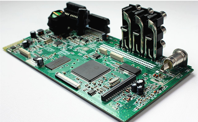
SMT patch requirements for BGA pad design
1. The center of the pad of each solder ball on the PCB coincides with the center of the corresponding solder ball at the bottom of the BGA.
2. The PCB land pattern is a solid circle, and the via hole cannot be processed on the land.
3. After the via hole is electroplated, it must be blocked with dielectric materials or conductive glue, and the height must not exceed the height of the pad.
4. Generally, the diameter of the pad is less than 20% to 25% of the diameter of the solder ball. The larger the pad, the smaller the wiring space between the two pads.
5. The number of wiring between two pads is calculated as P-D≥(2N+I)Xr where P is the pitch of the solder balls: D is the diameter of the pad: N is the number of wiring: X is the line width
6. General rule: The diameter of the pad of the PBGA is the same as the pad on the device substrate.
7. The width of the wire connected to the pad should be the same, generally 0.15~02mm.

8. The solder mask size is 0.1~0.15mm larger than the pad size. The print volume is greater than or equal to 0.08mm2 (this is the minimum requirement) to ensure the reliability of the solder joints after PCBA processing products. Therefore, the pad of CBGA is larger than that of PBGA.
10. Set the positioning line of the outer frame.
PCB processing bga welding
For more than ten years, because AOI can improve the fault detection speed and accuracy of PCB circuit board production, it has effectively strengthened process quality control. Improve product quality, increase inspection speed, and solve bottlenecks in the production process. Many customers regard whether the SMT production line is equipped with AOI as the symbolic testing equipment for quality assurance. AOI does bring benefits to the enterprise from many aspects such as quality, efficiency, cost, and corporate image. Therefore, many companies in the industry track the development of international SMT technology, and in recent years have successively launched AOI products with various advantages and various characteristics. And the automatic optical inspection equipment used for PCB assembly inspection is compared with the equipment launched several years ago.
Causes fragile solder joints and leads to service problems for the entire system. -Set the soldering iron at a reasonable temperature. I know it is tempting to keep improving the iron to increase efficiency, but you may be the shocking component. Even if lead-free solder is used, any temperature over 700oF (371oC) will run the risk of thermally stressing the component. If you find it necessary to keep the temperature elevated throughout the day, please refer to Tip #1. -If there are multiple components on a single component that need to be replaced, or the components are particularly sensitive to heat, a PCB preheater can be used. The preheater allows you to increase the temperature of the circuit board and maintain the temperature while working. Although the preheating temperature is much lower than the melting point of the solder, since you have not added it quickly from the ambient temperature, the thermal shock to the component can be minimized. Desoldering braids usually come in several different widths, so you can match the braiding to your desoldering. A wick that is too thin cannot remove enough solder and needs to be trimmed and remelted over and over again.
For multi-variety, small-batch production, customers are also very concerned about its comprehensive functions. The larger the range of PCB components that can be tested, the better. AOI equipment selects a single product according to the product object, and mass repeated production requires AOI, fast speed, combination of optical lenses on the hardware, and misjudgment of the length of the software; whether the programming and operating skills are easy to master, the self-learning function of the equipment, etc. AOI equipment’s misjudgment rate and miss-judgment rate are worth pointing out that the misjudgment rate/missing-judgment rate of the AOI system is related to many factors, such as resolution, degree of intelligence, pattern recognition and processing functions, etc., and more importantly programmers The empirical factors, the criteria for determining qualified/unqualified by programmers to adapt to various changes and conventional production conditions in a certain program are the main factors affecting misjudgment/missing judgment. For example: the same PCB component, how different color implementations are compatible for feature description, etc., is a typical example of easy misjudgment. The network interface of AOI equipment follows the development of information manufacturing and the expansion of enterprise scale.