Recently, I went to a comprehensive camera development and manufacturer to visit the whole production process of J-CAM. From appearance design, circuit board, precision mold design and manufacturing, injection molding, dust-free workshop oil injection, circuit board SMT high-speed patch, plug-in, assembly, testing, and packaging.
An excellent camera not only needs to have excellent results, but also an attractive appearance. A successful appearance design requires an excellent design concept, but to embody this concept in concrete objects, it also requires exquisite craftsmanship.
Design 1. Appearance design According to the Fanyi PCB design team, the pre-design work of the camera is also very complicated.
The birth of a new camera was originally inspired by a designer. The designer first sketched by hand, and roughly embodied his ideas on paper, drawing a simple general appearance.
After the ID team’s discussion and decision, use Rhino Rhino industrial modeling software to draw a few three-dimensional appearance renderings. After the discussion is roughly confirmed, the rough appearance drawing file is sent to the patterning center for CNC three-dimensional engraving. ", then review the physical model, and then continue to modify it according to the model designer. This process is to confirm the final appearance of the camera. After the appearance proofing, structure demonstration and design work will be carried out, generally used
"PRO-E" software, structural design.
When designing the base, many samples were made. According to market research, the designer found that most of the camera bases are "clips". This type of clip can be used to clip a notebook, but many of them cannot be clipped on the LCD with a very individual design. Some are too thick. The reason is that the backplane is irregular. The designer specially designed a universal "hanging stand", which is a base designed according to the principle of mechanics. It can be easily hung on laptops and LCD monitors without clips, and can also be placed on desktops or CRT monitors. This "hanging seat" is very energy intensive. I have done a lot of discussions with the mold designer on the materials, how the mold should be designed, and how to draw the mold, and I have also typed a lot of prototypes for experimentation. In the structural design stage, a wealth of mold knowledge and a lot of communication with mold designers are required.
The specific internal size is determined. At that time, the designer can give the size of the PCB board to the hardware engineer. At the same time as the design, the PCB design is also being carried out synchronously from now on, and a lot of communication must be done between each other, sometimes in order to compete A little bit of space, scolding each other with blushing ears.
In order to check the fit between the structure size and the PCB board, a structural prototype must be made. After testing, if there is a problem with the appearance or the internal structure does not match the PCB board, then modify it. Modifying the appearance is actually an iterative process. Until all the designs have reached the best fit and the mold is finally determined, then the PRO-E drawings will be officially submitted to the professional mold factory to make the mold. From appearance to structure, this design has taken the longest time, and there are many uncertain factors. It usually takes two to three months, and then it will get up soon.
Process of appearance design: 1. Inspiration: hand-drawn sketch
Confirm the general appearance 2. Practice: draw the general appearance with software pro-e or rhino 3. Initial color confirmation: use 3D
MAX for rendering 4. Use pro-e to make the internal structure to achieve the appearance needed 5. Make a hand version, purpose: confirm the appearance, check the structure and the PCB6. Modify the structure diagram 7. Make the mold (about 30 days)

2. The design of the PCB board. While the internal structure of the appearance is determined, the hardware engineer can
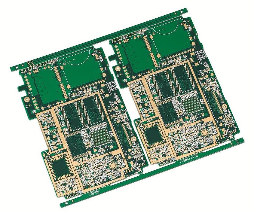
According to the given internal structure size, draw the schematic diagram. The first is to determine the plan, because the camera has a variety of options to choose from, so we must first determine the plan. Then you can use POWER PCB software to start drawing the schematic diagram.
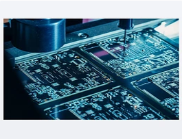
After the schematic diagram is drawn, convert it into a netlist, and then import the netlist into POWERPCB in POWERPCB, and make it into a PCB file. Then start drawing the PCB board frame, and first determine some fixed positions required by the mold, such as positioning holes, lights, and power sockets. Then layout and route the PCB board. The layout is mainly to ensure that the high-power components must be separated from each other, and the filter capacitor must be close to the corresponding IC pin. The main consideration for wiring is: the power and ground wires should be as thick as possible, and the wires that are easily interfered should be protected.
Then it is to sort out the BOM table, according to the schematic diagram, to see if there are any missing and extra components. After the check is correct, the prototype can be issued. There is a certain period of time for the manufacture of the prototype. After the manufacture is completed, it will be returned to the hardware engineer for component placement and debugging. Debugging is to see the effect. If the effect is not satisfactory, continue to modify and debug to achieve the best effect repeatedly.
The general design process: 1. Determine the plan, such as Vimicro 7131R+301L, or Micron + Songhan 120, etc. 2. Draw the schematic diagram according to the plan 3. Lead the schematic diagram into a PCB file 4. Draw the PCB frame and its mold The required fixed position. 5. Layout and wiring the PCB board. 6. Organize the BOM table. 7. After the inspection is correct, send the prototype. 8. After the prototype is returned, paste the components, and then debug. 9. After the debugging is correct, start production