SMT production line, surface mount technology (SurfaceMountTechnology for short SMT) is a new generation of electronic assembly technology developed from hybrid integrated circuit technology. It is characterized by the use of component surface mount technology and reflow soldering technology, which has become a new generation of electronic product manufacturing. Assembly technology.
The wide application of SMT has promoted the miniaturization and multi-function of electronic products, and has provided conditions for mass production and low defect rate production. It is surface assembly technology, a new generation of electronic assembly technology developed from hybrid integrated circuit technology.
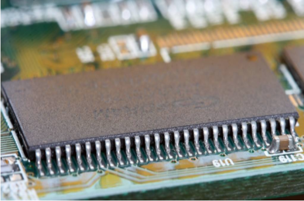
The main components of the SMT production line are: surface mount components, circuit substrates, assembly design, and assembly process;
The main production equipment includes printing presses, glue dispensers, placement machines, reflow soldering furnaces and wave soldering machines. Auxiliary equipment includes testing equipment, repair equipment, cleaning equipment, drying equipment and material storage equipment.
1. According to the degree of automation, it can be divided into fully automatic production lines and semi-automatic production lines;
2. According to the scale of the production line, it can be divided into large, medium and small production lines.

1. SMT basic process composition
Screen printing (or glue dispensing)>mounting>(curing)>reflow soldering>cleaning>testing>rework
2. SMT production process
1. Surface mount technology
1. Single-side assembly: (all surface mount components are on one side of the PCB)
Incoming inspection-solder paste mixing-screen printing solder paste-patch-reflow soldering 2. double-sided assembly; (surface mount components are on the A and B sides of the PCB respectively)
Incoming inspection-PCB A side silk screen solder paste-SMD-A side reflow soldering-flip board-PCB B side silk screen solder paste-SMD-B side reflow soldering-(cleaning)-inspection-rework
2. Mixed packaging process
1. Single-side mixed assembly process: (plug-ins and surface mount components are all on the A side of the PCB)
Incoming material inspection-solder paste mixing-PCB A side silk screen solder paste-SMD-A side reflow soldering-PCB A side plug-in-wave soldering or dip soldering (a small number of plug-ins can be manually soldered)-(cleaning)-inspection- Rework (post and insert)
2. Double-sided mixed packaging process:
(Surface mount components are on the A side of the PCB, and the plug-in is on the B side of the PCB)
A. Incoming inspection-solder paste mixing-PCB A side screen printing solder paste-SMD-reflow soldering-PCB B side plug-in-wave soldering (a small number of plug-ins can be manually soldered)-(cleaning)-inspection-repair
B. Incoming inspection-PCB A side silk screen solder paste-SMD-manual solder paste to the pad point of the plug-in on the A side of the PCB-PCB B side plug-in-reflow soldering-(cleaning)-inspection-rework
(Surface mount components are on the A and B sides of the PCB, and the plug-ins are on either side or both sides of the PCB)
First, perform the reflow soldering of the surface-mounted components on the A and B sides of the double-sided PCB according to the double-sided assembly method, and then perform the manual soldering of the plug-ins on both sides.
PCB
3. Introduction of SMT process equipment
1. Template: (Steel Mesh)
First, determine whether to process the template according to the design of the PCB. If the SMD components on the PCB are only resistors, capacitors, and the package is 1206 or more, you do not need to make a template, and use a syringe or automatic dispensing equipment for solder paste coating; when the PCB contains SOT, SOP, PQFP, PLCC and BGA packaged chips, resistors, and capacitors must be made into templates for packages below 0805. General templates are divided into chemically etched copper templates (low price, suitable for small batches, tests, and chip pin spacing 0.635mm); laser-etched stainless steel templates (high precision, high price, suitable for large-volume, automatic production lines and chip pin spacing) 0.5mm). For R&D, small batch production or 0.5mm spacing, it is recommended to use etched stainless steel templates; for mass production or 0.5mm spacing, use laser-cut stainless steel templates. The external size is 370*470 (unit: mm), and the effective area is 300*400 (unit: mm).
2. Silk screen: (High-precision semi-automatic solder paste printing machine)
Its function is to use a squeegee to print the solder paste or patch glue onto the pads of the PCB to prepare for the placement of the components. The equipment used is a manual screen printing table (screen printing machine), template and scraper (metal or rubber), located at the forefront of the SMT production line. It is recommended to use a medium-sized screen printing table and a precision semi-automatic screen printing machine to fix the template on the screen printing table. Use the up and down and left and right knobs on the manual screen printing table to determine the position of the PCB on the screen printing platform, and fix this position; The applied PCB is placed between the screen printing platform and the template, and solder paste is placed on the screen (at room temperature), keeping the template and PCB parallel, and evenly spreading the solder paste on the PCB with a scraper. In the process of use, pay attention to timely cleaning the template with alcohol to prevent the solder paste from clogging the leakage holes of the template.
3. Placement: (Korea high-precision automatic multi-function placement machine)
Its function is to accurately install the surface mount components on the fixed position of the PCB. The equipment used is a placement machine (automatic, semi-automatic or manual), vacuum suction pen or tweezers, located behind the screen printing table in the SMT production line. For the laboratory or small batches, it is generally recommended to use a double-tip anti-static vacuum suction pen. In order to solve the problem of placement and alignment of high-precision chips (chip pin spacing 0.5mm), it is recommended to use South Korea's Samsung automatic multi-function high-precision placement machine (model SM421 can improve efficiency and placement accuracy). The vacuum suction pen can directly pick up resistors, capacitors and chips from the component material rack. Because the solder paste has a certain viscosity, it can be directly placed on the required position for resistors and capacitors; for chips, a suction cup can be added to the vacuum suction pen tip. The suction power can be adjusted by the knob. Remember that no matter what kind of components are placed, pay attention to the alignment position. If the positions are misaligned, you must clean the PCB with alcohol, re-screen and re-position the components.
4. Reflow soldering:
Its function is to melt the solder paste, so that the surface mount components and the PCB are firmly brazed to achieve the electrical performance required by the design and are precisely controlled in accordance with the international standard curve, which can effectively prevent thermal damage and deformation of the PCB and components . The equipment used is a reflow oven (automatic infrared hot air reflow oven), located behind the placement machine in the SMT production line.
5. Cleaning:
Its function is to remove the substances that affect the electrical performance of the mounted PCB or solder residues such as flux, etc., if no-clean solder is used, it generally does not need to be cleaned. Products that require micro-power consumption or products with good high-frequency characteristics should be cleaned, and general products can be cleaned-free. The equipment used is an ultrasonic cleaning machine or directly manually cleaned with alcohol, and the position can be not fixed.
6. Inspection:
Its function is to inspect the soldering quality and assembly quality of the mounted PCB. The equipment used is a magnifying glass and a microscope, and the position can be configured in a suitable place of the production line according to the needs of the inspection.
7. Repair:
Its function is to rework PCBs that have detected faults, such as solder balls, solder bridges, and open circuits. The tools used are smart soldering irons, rework workstations, etc. Configured at any position in the production line.
Fourth, SMT auxiliary process: mainly used to solve the mixed process of wave soldering and reflow soldering.
1. Printing red glue: (red glue can be printed at the same time)
The function is to print the red rubber on the fixed position of the PCB. The main function is to fix the components on the PCB. Generally, it is used for both sides of the PCB with surface mount components and one side for wave soldering. The equipment used is a printer, solder paste and red glue printing can be done by one machine, located at the forefront of the SMT production line.
2. Curing: (reflow soldering is better for curing and leaded solder paste)
Its function is to cure the patch adhesive by heating, so that the surface mount components and the PCB are firmly bonded together. The equipment used is a curing oven (the reflow oven can also be used for the curing of glue and the thermal aging test of components and PCB), located behind the placement machine in the SMT production line.