PCB design of electronic products is a relatively cumbersome task. It must be planned well to achieve a multiplier effect with half the effort. If there is no process, it will be very tiring to work. The PCB design process generally has the following processes to share with you.
The basic process of PCB board design
First, clarify the design requirements of the PCB board. Electronic design comes from demand, and only when the demand is clear can the future process be determined. Be sure to communicate the detailed requirements with the product manager or the customer and sign for confirmation to prevent the requirements from being modified during the design process. A small requirement change may cause the entire design plan to be overturned.
Develop technical plans and chip selection. After the requirements are clarified, the technical solution is designed. When designing the technical solution, several more solutions should be made as a backup, and the advantages and disadvantages of each solution should be compared from the aspects of PCB board cost, production process, and design cycle for discussion.
Technical plan review. After taking out the technical plan, organize product managers, department leaders, and related colleagues to review. Technologists generally hate reviews and think that reviews can't play the role they should have. In fact, the purpose of the technical plan review is to determine the technical plan after everyone has unanimously confirmed it. If the technical plan cannot be implemented or overturned in the future, it will not put all the pressure and responsibility on one person.
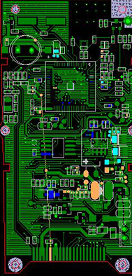
Design circuit and PCB layout. After the technical plan was determined, the implementation began. This stage includes the design of the schematic diagram of the PCB board the drawing of the component library, the design of the device package,PCB layout, etc. If necessary, you can organize colleagues to review and discuss technical details. The purpose of this discussion is to find problems in the circuit design process.

PCB board proofing and debugging, product testing. After the PCB template comes back, take the time to solder, debug the hardware circuit, debug the program, and draw the flowchart when programming. After the function comes out, test the model according to the test plan.
Prepare certification materials and process documents. After the product test is completed, it is necessary to prepare for the related work of product certification and evidence collection, and prepare the process documents to facilitate other colleagues to prepare for small-batch mass production.
The above is the general process of electronic product design. It should be noted that in the links that need to be discussed, it must be recorded and signed to prevent the situation of dumping the pot.
How to design a good PCB board
To design a good PCB board, roughly need the following steps:
Plan the layer and the definition of each layer. In addition to two-layer boards, four-layer boards, six-layer boards, or even more layers may be required. At the beginning of the design, it is necessary to determine the design of several layers and plan the definition of each layer;
Consider the layout of components. A good layout of components plays a vital role in the performance and stability of the product. When placing the components, place the components according to the function, signal flow direction, high and low voltage, etc.;
Requirements for wiring. Especially for radio frequency circuits and high-speed boards, wiring and routing are very critical; the handling of grounding. The processing of the ground wire is also very critical, and a lot of interference is introduced through the ground wire. When grounding at each point, consider choosing multi-point grounding or single-point grounding.
PCB board design is a very systematic work, and different circuits have different considerations, and specific situations require specific analysis.