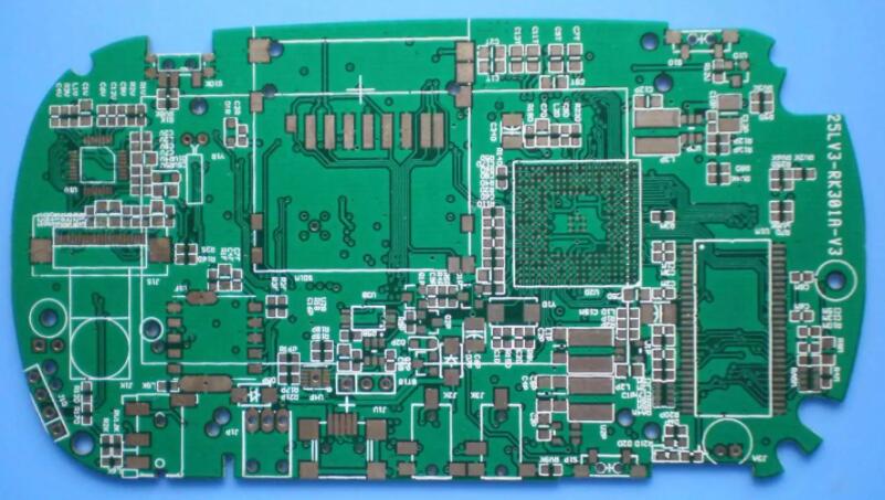
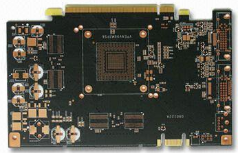
PCB circuit board copy board schematic diagram common mistakes

1. Common mistakes in PCB schematics:
(1) There is no signal connected to the ERC report pin:
A. I/O attributes are defined for the pins when the package is created;
B. Modify the inconsistent grid attributes when creating components or placing components, and the pins and lines are not connected;
C. When creating a component, the pin direction is reversed, and it must be connected to the non-pin name end.
(2) The component went out of the drawing boundary: no component was created in the center of the diagram paper in the component library.
(3) The network table of the project file created can only be partially imported into the PCB: when generating the netlist, it is not selected as global.
(4) When using multi-part components created by yourself, do not use annotate.
2. Common errors in PCB:
(1) It is reported that NODE is not found when loading the network:
A. The components in the schematic diagram use packages that are not in the PCB library;
B. The components in the schematic diagram use packages with inconsistent names in the PCB library;
C. The components in the schematic diagram use packages with inconsistent pin numbers in the PCB library. For example, a triode: the pinnumber in sch is e, b, c, and the pin number in PCB is 1, 2, 3.
(2) It can't always be printed on one page when printing:
A. It is not at the origin when creating the PCB library;
B. The component has been moved and rotated many times, and there are hidden characters outside the boundary of the PCB board. Choose to show all hidden characters, shrink the PCB, and then move the characters to the boundary.
(3) The DRC reporting network is divided into several parts:
means that this network is not connected. Look at the report file and use CONNECTEDCOPPER to find it.
In addition, remind friends to use WIN2000 as much as possible to reduce the chance of blue screen; export the file several times to make a new DDB file to reduce the file size and the chance of PROTEL freezing. If you make a more complicated design, try not to use automatic wiring.
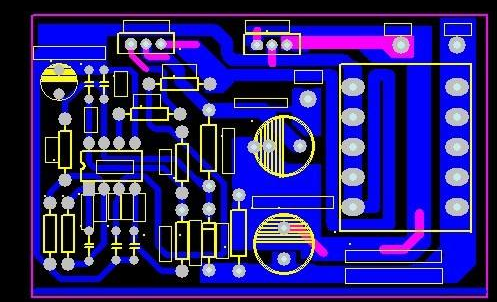
In PCB design, wiring is an important step to complete product design. It can be said that the previous preparations are done for it. In the entire PCB, the wiring design process is the most limited, the skills are the smallest, and the workload is the largest. PCB wiring includes single-sided wiring, double-sided wiring and multilayer wiring.
There are also two ways of wiring: automatic wiring and interactive wiring. Before automatic wiring, you can use interactive to pre-wire the more stringent lines. The edges of the input end and the output end should be avoided adjacent to parallel to avoid reflection interference.
Ground wire isolation should be added when necessary, and the wiring of two adjacent layers should be perpendicular to each other. Parasitic coupling is likely to occur in parallel.