1. Causes of SI problems
A common SI problem is reflection, and we know that PCB board transmission lines have the property of "characteristic impedance", which occurs when the "characteristic impedance" of different parts of the interconnect link does not match.
SI reflection problem in signal waveform representation is: upsurge/downsurge/ringing, etc.
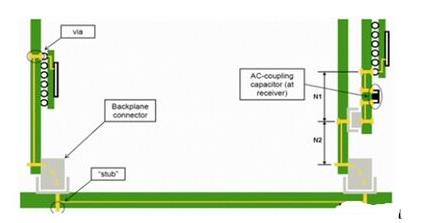
The following figure shows a typical high-speed signal interconnection link. The signal transmission path includes: 1. transmitter chip (package and PCB through hole)2. PCB cabling of child card 3. PCB cabling of child card 4. PCB cabling of backplane 5. Peer card connector 6. PCB cabling of peer card 7. AC coupling capacitance 8. Receiver chip (package and PCB through hole)

FIG 1. typical high-speed signal interconnection link
It can be seen that the high-speed signal interconnection link of actual electronic products is relatively complex, and impedance mismatch usually occurs at the connection points of different components, resulting in signal emission.
Common impedance discontinuities of high-speed interconnected links:
(1) Chip packaging: usually PCB wiring width in chip packaging substrate is much thinner than ordinary PCB board, impedance control is not easy;
(2) PCB through hole: PCB through hole is usually capacitive effect, low characteristic impedance, PCB design should pay attention to and optimization;
(3) connector: the design of the copper interconnection link in the connector should be simultaneously affected by both mechanical reliability and electrical performance, so as to seek a balance between the two;
PCB wiring, on the other hand, impedance control is generally easier than other interconnected components, focusing on the layered design, plate selection, but usually PCB processing board factory impedance control tolerance is 10%, to achieve 5-8% impedance tolerance control often requires higher processing costs.
2. Basic theory of transmission line reflection
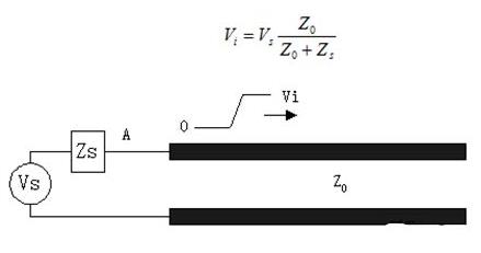
When a driver adds a signal to a transmission line, the amplitude of the signal depends on the voltage and resistance of the driver and the line impedance. The initial voltage on the driver is controlled by dividing the voltage between its own resistance and the impedance of the transmission line.
The following diagram depicts the initial waveform applied to a long transmission line. The initial voltage Vi is transmitted to the transmission line until it reaches the end. The amplitude of Vi is determined by the partial voltage of the driver resistance and the transmission line impedance:

FIG 2. Propagation of signal waveform in long transmission line
If the end of the transmission line is terminated by an impedance, and this impedance matches the impedance of the line, the signal of amplitude Vi will be terminated to the ground, and the voltage Vi will remain on line until the source is switched. In this case Vi is dc steady state. Otherwise, if the impedance at the end of the transmission line is not the characteristic impedance of the line, part of the signal ends to the ground, and the rest of the signal will be reflected back to the transmission line back to the source. The amount of signal reflected back is determined by the reflection coefficient, which is determined by the ratio of the reflected voltage to the input voltage at a given point. This point is defined as the impedance discontinuity on the transmission line. Impedance discontinuities can be part of a transmission line with different characteristic impedances, or they can be the end resistance or the input impedance to the chip buffer.
Where Z0 is the standard impedance of the transmission line, and Zt is the impedance of a discontinuous point on the transmission line.
The equation assumes that the signal transmitted on the transmission line with characteristic impedance Z0 encounters discontinuous impedance Zt. Note that if Z0=Zt, the reflection coefficient is 0, meaning there is no reflection. The case where Z0 is equal to Zt is called a matched end.
As shown in the figure below, when the input waveform is terminated with Zt, part of the signal Viρ is reflected back to the source and added to the input waveform, the amplitude of the whole input signal waveform is Viρ+Vi. The reflected part may produce another reflection from the source, and reflection and reflection continue until the transmission line is stable.

FIG 3. Signal reflection under impedance mismatch
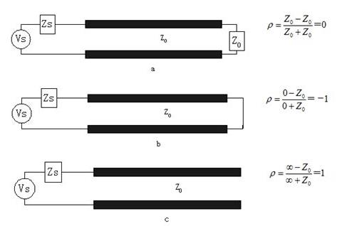
When the transmission line is fully matched, short-circuited and open, the reflection coefficient is shown as the figure below:

FIG 4. Reflection coefficients of (a) terminal (b) short circuit (c) open circuit
In the practical application of interconnection link, there is no ideal transmission line, it is impossible to match exactly, so the signal reflection is necessarily exist, the PCB design of the key lies in how to interconnect links parts of the impedance try to narrow the gap, so as to reduce the reflection signal amplitude, avoid multiple reflection lethal effects on the signal quality.