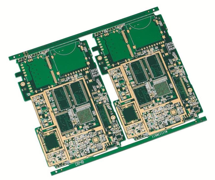
PCB board is the basic component of electronic products, and any electronic product needs to make PCB board. Then, PCB boards must be connected with other devices in electronic products, which is PCB board interconnection.
1. Interconnection between chip and PCB board
The problem of interconnection between chips and PCB boards is that the interconnection density is too high, which will lead to the basic structure of PCB materials becoming a factor limiting the growth of interconnection density. The solution is to use the local wireless transmitter inside the chip to transmit the data to the adjacent PCB board.

2. Internal interconnection
The internal interconnection of PCB board shall follow the following principles: use high-performance PCB board, whose insulation constants are controlled hierarchically to manage electromagnetic fields. Avoid the use of lead containing components, and avoid the use of through-hole processing on the sensitive plate, because this process will cause the wire inductance at the through-hole. Non chemical nickel plating or gold immersion plating process can provide better skin collection effect for high-frequency current.
3. External connection
External connections mainly include the following:
1) Wire welding
The external connection points on the printed board of the PCB can be directly welded with the components or other parts outside the board with wires, without any connectors.
2) Flat wire welding
This method is commonly used for the connection of two printed boards with an included angle of 90 degrees. After the connection, it becomes an integral PCB component.
3) Printed circuit boards socket
This connection mode is often used in more complex instruments and equipment. The printed plug is made from the edge of the PCB, and the plug part is designed according to the size of the socket, the number of connection points, the contact distance, the location of the positioning hole, etc., to make it match with the special PCB socket.
4) Standard pin connection
This method is suitable for use in small instruments. Two printed boards are connected by standard pins. The two printed boards are generally parallel or vertical.
4. Parallel PCB design plays an important role in PCB manufacturing industry
1) Collaborative work
Because PCB design is no longer a single person's work, but a team work between different engineer groups, communication has become one of the key issues in PCB design. Communication is the theme throughout the PCB design process. The circuit design team must clearly communicate their design intent to the PCB design team, and they must also clearly understand what their PCB design tools can and cannot do.
2) On the Design Principles of Parallel PCB
With the increase of PCB wiring complexity and signal rate, collaborative PCB design leads to better results than traditional serial processes. It has always been a common practice to isolate the design process of researching and selecting components, as well as the input, simulation, layout and routing stages of schematic diagrams. Therefore, it is better for design engineers to choose tools and processes that can promote data sharing, which is the only way for geographically dispersed design teams to take advantage of parallel work and shorten the overall design cycle.
a. The design cycle of traditional PCB serial development process is long, the information sharing is limited, and the cost continues to rise;
b. The parallel development process allows multiple development processes to be carried out synchronously, which helps to ensure the success of the design and avoid delays, additional costs and rework.
3) Design Creation
In the design and construction phase, the engineer finally determines the equipment and generates a library for it, which in turn speeds up the schematic diagram input. In this phase, the design engineer evaluates and selects building blocks, and can search for data tables and specifications on the manufacturer's website. A better method is to directly select the equipment during the schematic diagram input process, which can be used as a test method to achieve schematic diagram input. The above are the design principles that need to be followed for parallel PCB design in the production process.