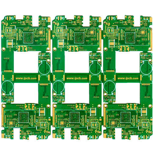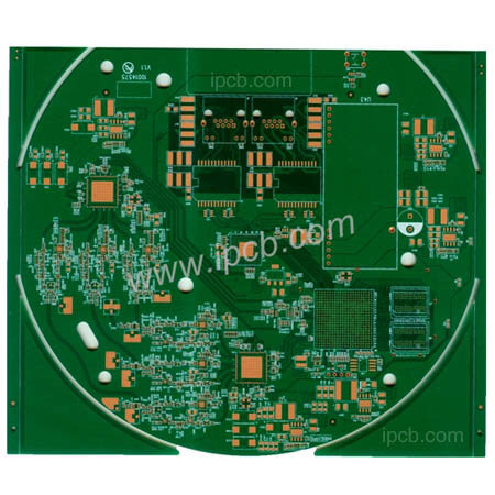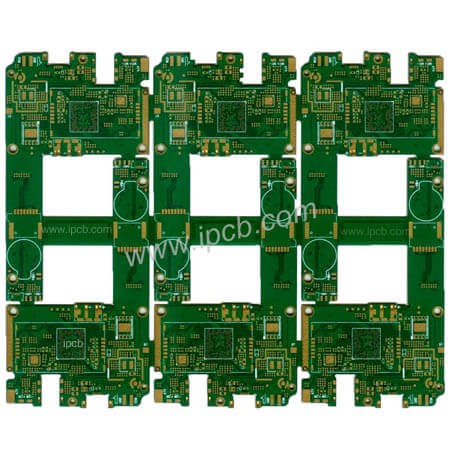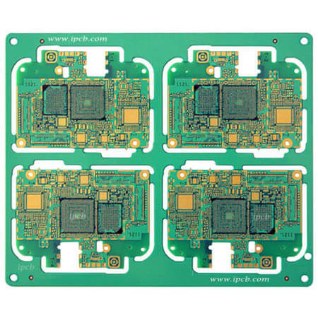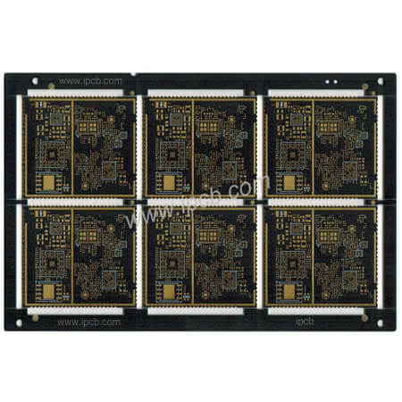
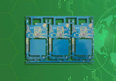

Model : 8Layers 2+N+2 HDI PCB
Material :FR-4
Layer :8L 2+N+2 HDI
Color :Blue/White
Finished Thickness:1.0mm
Copper Thickness :inner1OZ,outer0.5OZ
Surface Treatment :Immersion Gold
Min Trace / Space :3mil/3mil
Min Hole :Mechanical hole 0.2mm,Laser Hole 0.1mm
Application :Hand-held electronic equipment pcb
HDI is the English abbreviation of high density interconnect. It is a printed circuit board manufactured by high density interconnect (HDI). The printed circuit board is a structural element formed by insulating material and conductor wiring. When the printed circuit board is made into the final product, it will be equipped with integrated circuits, transistors (triodes, diodes), passive components (such as resistors, capacitors, connectors, etc.) and other various electronic parts. With the help of wire connection, electronic signal connection and due function can be formed. Therefore, the printed circuit board is a platform providing component connection, which is used to undertake the substrate of connecting parts.
Since the printed circuit board is not a general terminal product, the definition of the name is slightly confused. For example, the motherboard for personal computer is called the motherboard rather than the circuit board directly. Although there are circuit boards in the motherboard, they are different. Therefore, when evaluating the industry, the two are related but can not be said to be the same. Another example: because there are integrated circuit parts loaded on the circuit board, the news media call it integrated circuit board (IC board), but it is not equivalent to printed circuit board in essence.
On the premise that electronic products tend to be multi-functional and complex, the contact distance of integrated circuit components will be reduced, and the speed of signal transmission will be relatively improved. With the increase of the number of wiring and the local shortening of the length of wiring between points, it is necessary to apply high-density wiring configuration and micropore technology to achieve the goal. Wiring and jumper are basically difficult to achieve for single and double-sided boards, so the circuit board will move towards multi-layer. Due to the continuous increase of signal lines, more power layers and grounding layers are necessary means for design, which makes multi-layer printed circuit board more common.
For the electrical requirements of high-speed signal, the circuit board must provide impedance control with AC characteristics, high-frequency transmission capacity, reduce unnecessary radiation (EMI), etc. With the structure of stripline and microstrip, multi-layer design becomes necessary. In order to reduce the quality problem of signal transmission, insulating materials with low dielectric coefficient and low attenuation rate will be used. In order to cooperate with the miniaturization and array of electronic components, the density of circuit boards will be continuously increased to meet the demand. The emergence of BGA (ball grid array), CSP (chip scale package), DCA (direct chip attachment) and other group parts assembly methods has promoted the printed circuit board to an unprecedented high-density level.
Holes with a diameter of less than 150um are called microvia in the industry. The circuit made by using this microporous geometric structure technology can improve the efficiency of assembly, space utilization and so on. At the same time, it is also necessary for the miniaturization of electronic products.
For circuit board products with this structure, there have been many different names in the industry to call such circuit boards. For example, European and American companies used to call this kind of product SBU (sequence build up process), which is generally translated as "sequential layer adding method" because the program they produced is a sequential construction method. As for Japanese manufacturers, because the pore structure produced by such products is much smaller than that in the past, the manufacturing technology of such products is called MVP (micro via process), which is generally translated as "microporous process". Some people also call this kind of circuit board bum (build up multilayer board) because the traditional multilayer board is called MLB (multilayer board), which is generally translated as "add layer multilayer board".
Based on the consideration of avoiding confusion, the IPC circuit board Association of the United States proposed to call this kind of product technology the common name of HDI (high density interconnection) technology. If it is directly translated, it will become high density interconnection technology. However, this can not reflect the characteristics of the circuit board, so most circuit board manufacturers call this kind of product HDI board or the full Chinese name "high density interconnection technology". However, due to the problem of oral fluency, some people directly call this kind of product "high density circuit board" or HDI PCB board.
ipcb®.com Products:
Radio/Microwave/Hybrid High Frequency, FR4 Double/Multi-Layer, 1~3+N+3 HDI,Anylayer HDI, Rigid-Flex, Blind Buried, Blind Slot, Backdrilled,IC,Heavy Copper Board and etc.PCB apply for Industry 4.0, Communication, Industrial Control, Digital, Power supply, Computer, Automotive, Medical, Aerospace, Instruments, Military, Interne and other fields.
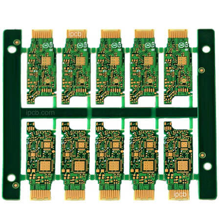
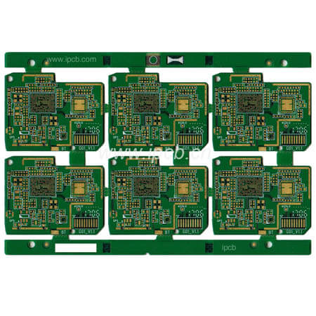
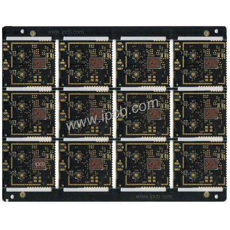
Model : 8Layers 2+N+2 HDI PCB
Material :FR-4
Layer :8L 2+N+2 HDI
Color :Blue/White
Finished Thickness:1.0mm
Copper Thickness :inner1OZ,outer0.5OZ
Surface Treatment :Immersion Gold
Min Trace / Space :3mil/3mil
Min Hole :Mechanical hole 0.2mm,Laser Hole 0.1mm
Application :Hand-held electronic equipment pcb
For PCB technical problems, iPCB knowledgeable support team is here to help you with every step. You can also request PCB quotation here. Please contact E-mail sales@ipcb.com
We will respond very quickly.