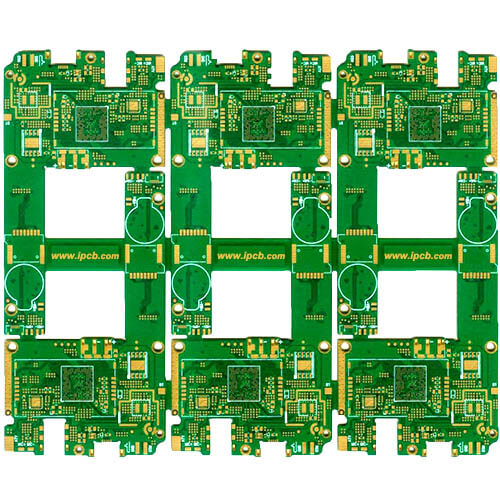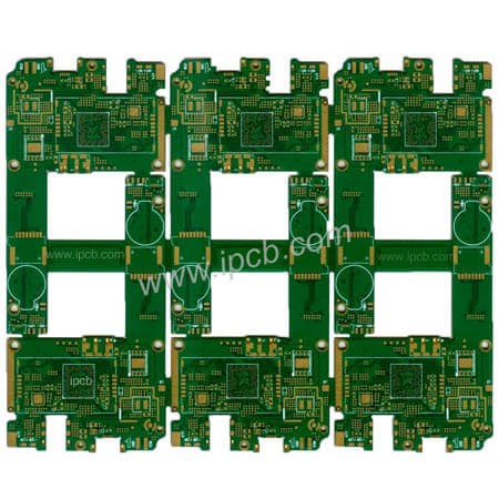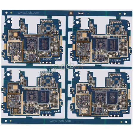
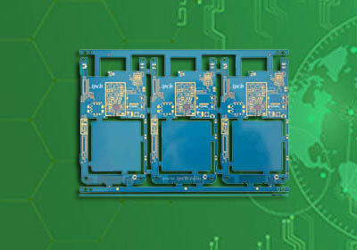


Model:Type-C Connector PCB
Material:High TG FR4
Construction:6Layers 2+N+2 HDI PCB
Finished Thickness:0.8mm
Copper Thickness :1OZ
Color:Green /White(PSR:TAIYO INK)
Surface Treatment:Immersion Gold+OSP
Min Trace / Space:3mil/3mil
Min Hole:Mechanical Hole0.2mm,Laser Hole0.1mm
Specail Process:The tolerance requirement of Outline &PSR Tolerance are stick
Application: type-c data and power transmission
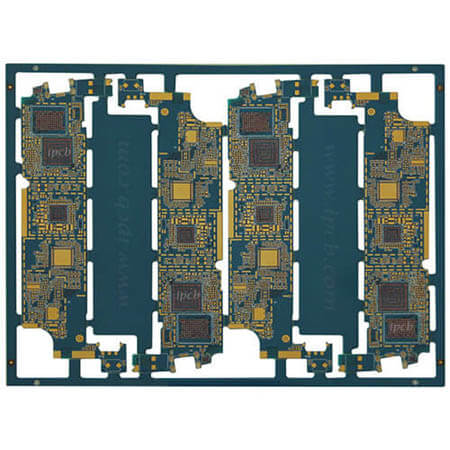
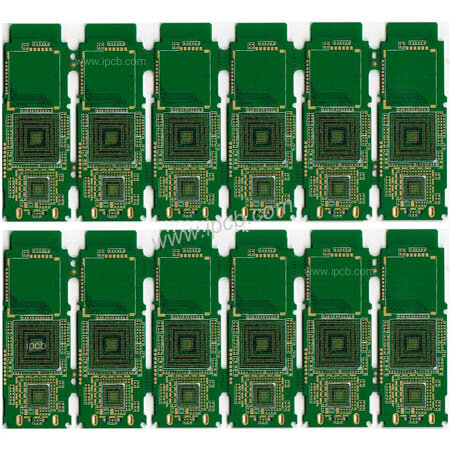
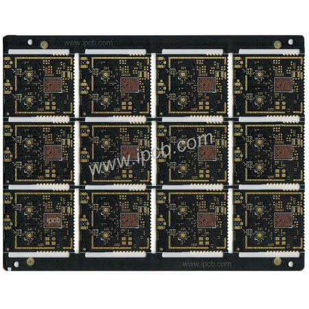
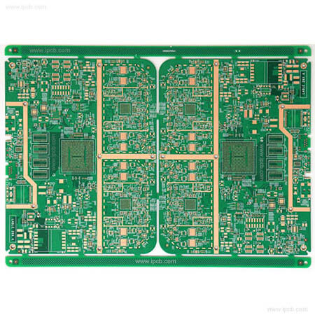
What Are HDI(High Density Interconnector)PCB?
A high density interconnector printed circuit board (HDI PCB) is a circuit board that has a higher wiring density per unit area as opposed to conventional circuit boards. This allows for more components to fit in the total available space. HDI PCBs are useful for increasing electrical performance while reducing the weight and size of equipment.
ipcb's HDI PCB Capabilities allows you to easily overcome the limitations found in standard circuit technologies through the utilization of ultra-thin cores, fine line processing and alternative via methods to reduce the size and weight of your components while simultaneously enhancing performance.
For some HDI PCB process capabilities, please refer to: HDI PCB Technics Capacity


Layer structure of 2 + N + 2 HDI PCB(1+n+1 = single layer of microvia, 2+n+2 = 2 layers of microvia, 3+n+3 = 3 layers of microvia, 4+n+3 = 4 layers of microvia, 5+n+5 = 5 layers of microvia, 5+n+5 = 5 layers of microvia)
The HDI PCBs ipcb offer include the following highly requested characteristics:
1. Through vias from surface to surface
2. Via-in-pad
3. Blind and/or buried vias
4. 30 µm dielectric layers
5. 20 µm circuit geometries
6. 50 µm laser vias
7. 125 µm bump pitch processing
Our high density circuit boards have the technology-pushing capabilities to drive applications in a large number of industries including but not limited to semiconductor test equipment, medical and aerospace.

*Send inquiry to sales@ipcb.com directly
*Any question,Don't hesitate to contact us through click "chat" button to get in touch with us.Or leave your contact info,We will get back to you as soon as possible.
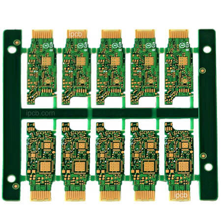
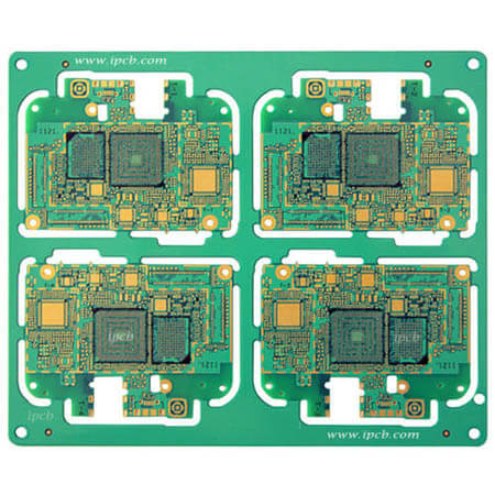
Model:Type-C Connector PCB
Material:High TG FR4
Construction:6Layers 2+N+2 HDI PCB
Finished Thickness:0.8mm
Copper Thickness :1OZ
Color:Green /White(PSR:TAIYO INK)
Surface Treatment:Immersion Gold+OSP
Min Trace / Space:3mil/3mil
Min Hole:Mechanical Hole0.2mm,Laser Hole0.1mm
Specail Process:The tolerance requirement of Outline &PSR Tolerance are stick
Application: type-c data and power transmission
For PCB technical problems, iPCB knowledgeable support team is here to help you with every step. You can also request PCB quotation here. Please contact E-mail sales@ipcb.com
We will respond very quickly.