

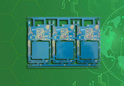

Model : 1+N+1 HDI PCB for Digital Product
Layers : 6Layers
Material : SY S1000-2 FR4
Construction : 1+4+1 HDI PCB
Finished Thickness:1.2mm
Copper Thickness : 0.5OZ
Color : Green/White
Surface Treatment:Immersion Gold
Min Trace / Space:4mil/4mil
Min Hole:Laser Hole 0.1mm
Application : Digital Product PCB
HDI PCB (high density interconnect board) is a kind of PCB with high line distribution density using micro blind buried hole technology. HDI PCB has inner circuit and outer circuit, and then uses the technology of drilling and metallization in hole to realize the internal connection of each layer circuit.
HDI PCB is usually manufactured by lamination method. The more times of lamination, the higher the technical grade of the plate. The common HDI PCB is basically a one-time build-up, while the high-order HDI uses two or more layers. At the same time, advanced PCB technologies such as stack hole, electroplating hole filling and laser direct drilling are used.
When the density of PCB increases more than eight layers, the cost of HDI manufacturing will be lower than that of traditional complex pressing process. HDI PCB is beneficial to the use of advanced construction technology, and its electrical performance and signal accuracy are higher than those of traditional PCB. In addition, HDI PCB has better improvement on radio frequency interference, electromagnetic wave interference, electrostatic discharge and heat conduction.
Electronic products continue to develop towards high density and high precision. The so-called "high" means not only improving the performance of the machine, but also reducing the volume of the machine. High density integration (HDI) technology can make terminal product design more miniaturized, while meeting higher standards of electronic performance and efficiency. At present, many popular electronic products, such as mobile phones, digital cameras, notebook computers, automobile electronics, etc., use HDI PCB. With the upgrading of electronic products and the market demand, the development of HDI PCB will be very rapid.
Model : 1+N+1 HDI PCB for Digital Product
Layers : 6Layers
Material : SY S1000-2 FR4
Construction : 1+4+1 HDI PCB
Finished Thickness:1.2mm
Copper Thickness : 0.5OZ
Color : Green/White
Surface Treatment:Immersion Gold
Min Trace / Space:4mil/4mil
Min Hole:Laser Hole 0.1mm
Application : Digital Product PCB
For PCB technical problems, iPCB knowledgeable support team is here to help you with every step. You can also request PCB quotation here. Please contact E-mail sales@ipcb.com
We will respond very quickly.


