

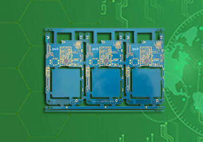

Model : HDI Mouse Bite PCB
Layers: 10Layer
Material: SY S1000-2
Construction : 1+4+q
Finished Thickness:0.8mm
Copper Thickness: 1OZ/1OZ
Color: Green/White
Surface treatment: ENIG
Min Trace / Space:3mil/3mil
Application: Consumer HDI PCB Board
Production process flow of HDI Mouse Bite PCB
HDI metal Mouse Bite (groove) refers to the second drilling and shape process after the first drilling hole is perforated, and finally, the metalized hole is retained (slot) half, that is, the metalized hole on the board edge is cut in half. In the PCB industry, it is also called a stamped hole. The hole edge can be directly welded with the main edge to save the connector and space. It often appears in the signal circuit. What is the production process flow of Mouse Bite PCB?
The production process flow of HDI Mouse Bite PCB includes the following steps:
1. Outer circuit design;
2. Base plate pattern electroplating copper;
3. Electro tinning of substrate pattern;
4. Half hole treatment;
5. Film removal;
6. Etching.
Process interpretation:
(1) How to control the product quality after forming the semi-metalized hole on the plate edge, such as the warping and residue of copper thorn on the hole wall, has always been a difficult problem in the processing process.
(2) For this kind of PCB with a whole row of semi-metalized holes on the edge of the board, the hole diameter is relatively small. Most of them are used for the daughter board of the motherboard and are welded with the pins of the motherboard and components through these holes. If there are copper thorns left in these semi-metalized holes when the manufacturer carries out welding, it will lead to loose welding feet and false welding, and seriously lead to a bridge short circuit between the two pins. Attention should be paid to details in the design of half orifice plate

HDI PCB half orifice:
Mouse Bitesize range: diameter ≥ 0.6mm, hole edge to hole edge ≥ 0.6mm, Here, someone will ask what is a half orifice? As shown in the figure
The definition of the metal half hole (groove) is that one drill hole is drilled and then another is drilled, and the shaping process is adopted to finally retain half of the metalized hole (groove), which is simply to cut half of the metalized hole at the plate edge, The semi metalized hole process of plate edge is a very mature process in IPCB.
How to control the product quality after forming the semi-metalized hole on the plate edge. For example, the cocking and residue of copper thorns on the hole wall has always been a difficult problem in the processing process.
This kind of PCB with a whole row of semi-metalized holes on the edge of the board is characterized by a small aperture, which is mostly used on the carrier board. As a daughter board of a motherboard, it is welded with the motherboard and the pins of components through these semi-metalized holes.
Therefore, if copper spikes remain in these semi-metalized holes when the plug-in manufacturer carries out welding, it will lead to loose welding feet, false welding, and seriously cause bridging short circuit between the two pins.
Whether drilling or milling, the rotation direction of the spindle (spindle) is clockwise. When the tool is processed to point a, the hole wall metallization layer of point a is closely connected with the substrate layer to prevent metal damage
The extension of the metallization layer during processing and the separation of the metallization layer from the hole wall will also ensure that there will be no copper thorn warping and residue after processing here; When the tool is processed to point B, due to the copper attached to the hole wall,
Without any adhesion support, when the tool runs forward, the metallization layer in the hole will curl with the rotation direction of the tool under the influence of external force, resulting in copper thorn warping and residue.

In the design of HDI Mouse Bite, try to place the pad to the area inside the plate frame line (hanging copper). It should be larger than the gongs empty area. It is often encountered that the half hole drawn by the customer is not standard, only one third of it
If the hole is in the plate, this design can not meet the production process. At least the pad has to divide the plate frame line equally.
It is emphasized that the half hole plate has one side, two sides, three sides and half holes, and four sides and mouse bite. The distance from the half hole pad to the four corners must be at least 2mm.

It is used as a clamping edge to connect the panel.iPCB will exceed one knife of the half hole on both sides of the milled (formed) half hole plate, so the plate connection position is smaller.
It is suggested that the half hole plate should not be made up. If it is necessary to make up, a (1.6-2.0) mm spacing should be added around the plate, and the half hole plate should be processed and shipped. The half hole plate can not be combined with the plate
For other plate assembly production, the order must be specially indicated.
Reasons for increasing the cost of HDI Mouse Biet PCB: Mouse Bite is a special process flow. In order to ensure that there is copper in the hole, it is necessary to make gongs and edges at half of the process, and generally
The Mouse Bite HDI PCB is very small, so the general cost of the half hole plate is relatively high, and the unconventional design has an unconventional price.
HDI Mouse Bite panel:
Here, we also apply the universal stamp hole splicing method, so as to build connecting ribs between small plates. In order to facilitate cutting, the ribs are placed on the small Printed Circuit Board.
There will be some small holes on the surface (the diameter of the conventional hole is 0.65-0.85mm), which is called the stamp hole.? because the current plates have to pass through the SMD machine, it is necessary to do so
When connecting the PCB, you can have too many PCBs at a time. After SMD, the plates should be separated. This stamp hole is set to make the plates easy to separate.
It is emphasized here that V-CUT forming is not allowed for the half hole edge, and it must be formed by gongs and hollows (CNC).
1. V-CUT splicing, and V-CUT forming is not performed at the edge of the half hole plate (copper wire will be pulled, resulting in no copper in the hole)
2. Spelling of stamp holes:
The HDI PCB splicing methods are mainly V-CUT, bridging and bridging stamp holes. The size of the [color = RGB (128, 184, 255)! Important] splicing can not be too large or too small,
Generally, small boards can be assembled for processing or welding.

1. The Mouse Bite template is not connected to the assembly, and can only be shipped in one piece
2. The Mouse Bite board below 10 * 10mm is not connected
3. Half orifice plate does not accept expediting
Model : HDI Mouse Bite PCB
Layers: 10Layer
Material: SY S1000-2
Construction : 1+4+q
Finished Thickness:0.8mm
Copper Thickness: 1OZ/1OZ
Color: Green/White
Surface treatment: ENIG
Min Trace / Space:3mil/3mil
Application: Consumer HDI PCB Board
For PCB technical problems, iPCB knowledgeable support team is here to help you with every step. You can also request PCB quotation here. Please contact E-mail sales@ipcb.com
We will respond very quickly.


