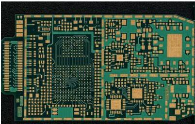
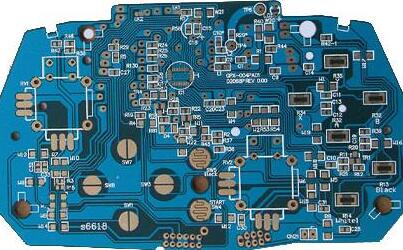
High-speed PCB board design is often overlooked or quite important. System board layout has become an integral part of the design itself, so it is important to understand the mechanisms that affect the performance of high-speed signal link designs. Despite being engineers, we are also likely to "create" more trouble. So don't get too picky and get CAD engineers bogged down with designs that don't bring any performance improvement. The exposed pad is sometimes overlooked, but it is very important to get the most out of the signal link and to help dissipate heat from the device. The exposed pad is commonly referred to as pin 0 at Analog Devices and is the pad underneath most devices today. It is an important contact through which all internal grounds of the chip are generally connected to the center point under the device. Have you noticed that many converters and amplifiers are missing a ground pin these days? The exposed pad is why. The key is to properly secure (i.e. solder) this pin to the printed circuit boards(PCB) with a robust electrical and thermal connection, otherwise the system design could suffer all kinds of damage.

Making electrical and thermal connections using the exposed pad is basically a three-step process. First, duplicate exposed pads on all layers of the PCB where possible, which will provide thicker thermal connections to all grounds and ground planes for fast heat dissipation. This step is relevant for high power devices and applications with multiple channels. Electrically, this will provide good equipotential bonding for all ground planes. You can even replicate the exposed pad on the bottom layer, which acts as a hot air pad ground point for decoupling and a place to mount the bottom side heat sink.
Second, divide the exposed pad into multiple identical parts like a checkerboard. This can be done in two ways: using screen printed cross-hatching or solder mask on the open exposed pad. This step ensures a robust connection between the device and the PCB. During the reflow assembly process, there is no certainty how the solder paste will flow and ultimately connect the device to the PCB. The problem that arises is that the connections may exist but not be evenly distributed. There may be only one connection and the connection is small, or worse, the connection is in the corner. Dividing the exposed pad into smaller sections ensures that each area has a connection point, resulting in a more robust, evenly connected exposed pad. It should be ensured that each section has vias connected to ground. Each area is usually large enough to place multiple vias. Be sure to fill each via with solder paste or epoxy prior to assembly. This step is very important to ensure that the exposed pad solder paste does not reflow into these via voids, reducing the chances of a proper connection. Sometimes we ignore the purpose of using decoupling and just spread many values of capacitors across the board so that the lower impedance power supply is connected to ground. But the question remains: how many capacitors are needed? Many literatures state that multiple capacitors and multiple values should be used to reduce the impedance of the power transmission system (PDS), but this is not entirely true. In fact, the impedance of the PDS can be reduced simply by choosing the correct value and the correct "kind" of capacitor. However, let's look at the green curve again, which uses only 0.1µF and 10µF capacitors on the same design. This proves that if you use the right capacitors, you don't need to use so many capacitor values. This also helps save on layout and bill of materials (BOM) costs. However, not all capacitors are "created equal", and even within the same supplier, there are differences in craftsmanship, size and style. If the correct capacitors are not used, whether multiple capacitors or several different types of capacitors are used, the result can be counterproductive to the PDS. The placement of capacitors or the use of different capacitor technologies and sizes can create inductive loops that will respond differently to frequencies within the system and resonate with each other. It is important to know the frequency response of the type of capacitor used in the system. A random choice of capacitors can undo the effort to design a low-impedance PDS system. To design a qualified PDS, various capacitors need to be used. Typical capacitor values used on PCBs only reduce impedance in the frequency range of about 500MHz at or near DC. Above 500MHz, the capacitance will be determined by the internal capacitance formed by the PCB. Are the power and ground planes stacked closely enough? To do this, design a PCB stack-up that supports larger planar capacitances. For example, a six-layer stack may include a top signal layer, a ground layer, a power layer, a second power layer, a second ground layer, and a bottom signal layer. The ground layer and the power supply layer are specified to be close to each other in the stacked structure. Setting the spacing of these two layers to 2~4mil will form an inherent high frequency planar capacitance. The beauty of this capacitor is that it, you just need to explain it in your PCB fabrication notes. If you must split the power plane and have multiple VDD supply rails on the same plane, use the largest possible power plane. Do not leave voids, while also being careful with sensitive circuits. This will allow the capacitance of the VDD plane to reach. If the design allows for extra layers (six instead of eight in this example), two extra ground planes should be placed between and the second power plane. In the case of the same 2~3mil spacing, the inherent capacitance of the stacked structure will be doubled (Figure 6). This structure is easier to design, then more discrete high frequency capacitors can be added to keep the impedance low.
Minimizing the voltage ripple that occurs in response to supply current demands is an important, but often overlooked, PDS for PDS. All circuits require current, some circuits require a large amount of current, and some circuits require current to be supplied at a faster rate. Voltage ripple due to circuit current demands can be minimized with a well-decoupled low-impedance power or ground plane and good PCB stack-up. According to the decoupling strategy used, if the switching current of the system design is 1A and the impedance of the PDS is 10mΩ, the voltage ripple is 10mV. The calculation formula is simple: V=IR. With a perfect PCB stack-up, the high frequency range can be covered, while the low frequency range (<500MHz) can be covered by using traditional decoupling at the starting entry point of the power plane and around high power or inrush current devices. This will ensure that the PDS impedance is constant over the entire frequency range. There's no need to put capacitors everywhere, and there's no need to break all the manufacturing rules in order to put capacitors right across each IC. If this kind of overshoot is required, then there are other problems in the circuit.
Some layouts inevitably have overlapping circuit planes. In some cases it may be a sensitive analog plane (be it power, ground, or signal), and the next layer is a noisy digital plane. Most designers don't think it matters because the plane is on another level. So let's do a simple test. Taking a layer as an example, inject signals on any plane. Now connect another layer cross-coupled with this adjacent layer to the spectrum analyzer. Can you see how many signals are coupled to adjacent layers? Even though the two are separated by 40 mils, it is still capacitive in the sense that it will still couple signals to adjacent planes at certain frequencies. For example, a high-noise digital plane on one layer has a 1V signal switching at high speed, which means that another layer will "see" 1mV of coupling (about 60dB of isolation). For a 12-bit analog-to-digital converter (ADC) with a 2Vp-p full-scale swing, this is a coupling of 2 significant bits (LSBs). For certain systems this may not be a problem, but it should be noted that if you boost by 2 bits (from 12 to 14 bits), the sensitivity will only increase by a factor of four, or 8 LSBs. Neglecting this inter-plane coupling is likely to fail the system or affect design performance. It must be pointed out here that the coupling between the two planes may be beyond imagination. This should be noted when noise coupling is found within the spectrum of interest. Sometimes layout dictates that unintended signals or planes will be cross-coupled to different layers, keep this in mind when debugging sensitive systems. The problem may appear one level below.
A common question asked by analog signal chain designers is, should the ground plane be separated into AGND and DGND ground planes when using an ADC? The short answer is: it depends. The detailed answer is: usually not separate. In most cases, blindly separating the ground plane will only increase the inductance of the return current, so it does more harm than good. Remember the formula V=L(di/dt)? As the inductance increases, the voltage noise increases. As the inductance increases, so does the PDS impedance you've been trying to reduce. As the need to increase ADC sampling rates continues to grow, there are only so many ways to increase switch current. So unless there is a reason to separate the ground planes, keep these ground connections.
The key is to divide the circuit properly so that the ground plane does not have to be separated. Note that there is no need to separate ground planes if the layout allows the circuits to be kept in their own area. This division provides a star ground and, therefore, confines the return current to a specific portion of the circuit. For example, size constraints make it impossible to achieve good layout partitioning of the board. This may be due to the fact that harsh bus power supplies or noisy digital circuits must be placed in specific areas to comply with legacy design or size requirements. In this case, separating the ground plane is the key to good performance. However, for the overall design to be effective, these grounds must also be connected together with a bridge or junction somewhere on the board. Therefore, the connection points should be distributed evenly on separate ground planes. Connection points on the PCB tend to be locations where return currents can pass without degrading performance or forcibly coupling the return currents to sensitive circuits. If this connection point is near or below the converter, there is no need to separate the ground at all.
With so many comments about the layout, it's always confusing to think about the layout. Technology and principles have always been part of ADI's "Design Culture". While engineers tend to draw on past design experience, the pressure to market a product also discourages designers from changing or trying new things. They stick to risk trade-offs until a major problem occurs within the system. At the evaluation board, module, and system level, a simple single ground is suitable for all situations. Good circuit partitioning is the key, which will also affect the layout of the plane and adjacent layers. Note that cross-coupling is possible if the sensitive plane is above the noisy digital plane. Assembly is also an important factor. Manufacturing notes provided to the PCB shop or assembly shop should be put to good use to ensure a reliable connection between the IC's exposed pad and the PCB. Countless systems can suffer from poor system performance due to poor assembly. However, decoupling close to the power plane entry point and the converter VDD pin is always beneficial. For increased, inherently high frequency decoupling, use tight power and ground planes with 4 mils or less apart. There is no additional cost to this method, and it only takes five minutes to update your PCB fabrication notes. Not all specific characteristics can be accounted for when designing a high-speed, high-resolution converter layout. Every app is different, and some are even more unique. However, the above key points can help designers deepen their understanding of future system design on
PCB board.