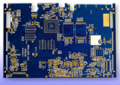
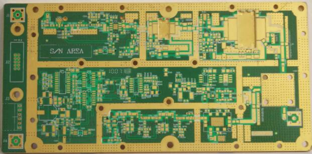
High-frequency PCB board is defined as a circuit board with a frequency above 1GHz, with very high requirements for various physical properties, accuracy, and technical parameters. It is often used in automotive anti-collision systems, satellite systems, radio systems and other fields. The high-frequency PCB board is an important link in the wiring, which directly affects the high-frequency and high-speed operation. Today I will talk about how to wire high-frequency and high-speed PCB boards.
How should the high frequency circuit board be wired?
Pay special attention to the wiring of high-frequency circuit boards. Based on the basic knowledge of microwave technology, when the wavelength of the signal is small enough to be proportional to the length of the transmission line, we cannot analyze the circuit according to the traditional lumped circuit method, but use the field The theoretical analysis, this is the transmission line theory. Of course, under normal circumstances, the signal frequency of the circuit we design will not be too high. Wavelength = signal transmission speed/signal frequency. Generally, the transmission speed of the signal is related to the dielectric constant of the transmission medium. We might as well set the signal transmission speed as the speed of light. 3*10^8m/s (actually less than) For 300Mhz signals, the wavelength is 1m, and usually the line length on the PCB board will not reach 1m. It can be seen that we don't have to worry too much about signals with low frequencies.

What are the high frequency PCB wiring requirements?
When the signal frequency of the high-frequency PCB board is high, in order to reduce the reflection of the signal, impedance matching is required on the transmission line. Generally, the single-ended line can be used for remote matching or terminal matching, and the differential signal is usually bridged between the differential lines near the terminal. Resistance matching. As far as my recent topic is concerned, the transmission of LVDS signals on differential lines requires a 100 ohm resistor to be placed on the receiving end for impedance matching. According to the knowledge of the transmission line, the characteristic impedance of the differential line must be 100 ohms to be completely matched. For this reason, the line width and line spacing of the differential line have strict requirements. The characteristic impedance of the differential line is related to the dielectric constant of the substrate, the thickness of the substrate, the copper thickness of the wire, the line width of the differential line, the line distance of the differential line, the thickness of the green oil of the substrate, etc. The calculation formula is also quite complicated.

High-frequency circuit board wiring skills
1. The less the lead layer alternate between the pins of the high-frequency circuit device, the better
The so-called "the less the inter-layer alternation of the leads, the better" means that the fewer vias (Via) used in the component connection process, the better. A via can bring about 0.5pF distributed capacitance, reducing the number of vias can significantly increase the speed and reduce the possibility of data errors.
2. The lead between the pins of high-speed electronic devices should be bent as little as possible
The lead wire of high-frequency circuit wiring is best to adopt a full straight line, which needs to be turned. It can be turned by a 45-degree broken line or a circular arc. This requirement is only used to improve the fixing strength of the copper foil in low-frequency circuits, while in high-frequency circuits, this requirement is met. One requirement can reduce the external emission and mutual coupling of high-frequency signals.
3. The shorter the lead between the pins of the high-frequency circuit device, the better
The radiation intensity of the signal is proportional to the trace length of the signal line. The longer the high-frequency signal lead, the easier it is to couple to the components close to it. Therefore, for signals such as clock, crystal oscillator, DDR data, LVDS lines, USB lines, HDMI lines and other high-frequency signal lines are required to be as short as possible.
High frequency PCB board wiring rules
First, high-frequency PCB board wiring needs to pay attention to the "crosstalk" introduced by the close parallel routing of the signal line
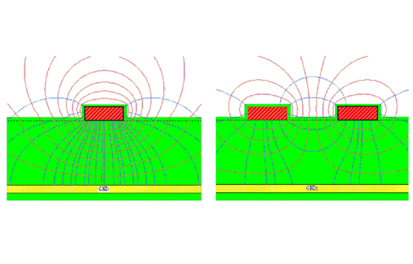
High-frequency circuit wiring should pay attention to the "crosstalk" introduced by the close parallel routing of signal lines. Crosstalk refers to the coupling phenomenon between signal lines that are not directly connected. Since high-frequency signals are transmitted in the form of electromagnetic waves along the transmission line, the signal line will act as an antenna, and the energy of the electromagnetic field will be emitted around the transmission line. Undesirable noise signals are generated due to the mutual coupling of electromagnetic fields between the signals. Called crosstalk (Crosstalk). The parameters of the PCB layer, the spacing of the signal lines, the electrical characteristics of the driving end and the receiving end, and the signal line termination method all have a certain impact on the crosstalk. Therefore, in order to reduce the crosstalk of high-frequency signals, it is required to do the following as much as possible when wiring:

(1) When the wiring space permits, insert a ground wire or ground plane between the two wires with more serious crosstalk, which can play a role of isolation and reduce crosstalk;
(2) When there is a time-varying electromagnetic field in the space surrounding the signal line, if parallel distribution cannot be avoided, a large area of "ground" can be arranged on the opposite side of the parallel signal line to greatly reduce interference;
(3) If the wiring space permits, increase the spacing between adjacent signal lines, reduce the parallel length of the signal lines, and try to make the clock line perpendicular to the key signal line instead of parallel;
(4) If parallel wiring in the same layer is almost unavoidable, in two adjacent layers, the direction of the wiring must be perpendicular to each other;
(5) In digital circuits, the usual clock signals are signals with fast edge changes, which have high external crosstalk. Therefore, in the design, the clock line should be surrounded by a ground wire and more ground wire holes should be used to reduce the distributed capacitance, thereby reducing crosstalk;
(6) For high-frequency signal clocks, try to use low-voltage differential clock signals and wrap the ground mode, and pay attention to the integrity of the ground punching;
(7) Do not suspend the unused input terminal, but ground it or connect it to the power supply (the power supply is also grounded in the high-frequency signal loop), because the dangling wire may be equivalent to the transmitting antenna, and the grounding can inhibit the transmission. Practice has proved that using this method to eliminate crosstalk can sometimes yield immediate results.

2. Isolate the ground wire of the high-frequency digital signal from the ground wire of the analog signal
When the analog ground wire, digital ground wire, etc. are connected to the public ground wire, use high-frequency choke magnetic beads to connect or directly isolate and select a suitable place for single-point interconnection. The ground potential of the ground wire of the high-frequency digital signal is generally inconsistent. There is often a certain voltage difference between the two directly. Moreover, the ground wire of the high-frequency digital signal often contains very rich harmonic components of the high-frequency signal. When the digital signal ground wire and the analog signal ground wire are directly connected, the harmonics of the high-frequency signal will interfere with the analog signal through the ground wire coupling. Therefore, under normal circumstances, the ground wire of the high-frequency digital signal and the ground wire of the analog signal are to be isolated, and a single-point interconnection method can be used at a suitable position, or a method of high-frequency choke magnetic bead interconnection can be used.
3. Add high-frequency decoupling capacitor to the power supply pin of the integrated circuit block
A high-frequency decoupling capacitor is added to the power supply pin of each integrated circuit block nearby. Increasing the high-frequency decoupling capacitor of the power supply pin can effectively suppress the interference caused by the high-frequency harmonics on the power supply pin.
Fourth, it is necessary to ensure good signal impedance matching
In the process of signal transmission, when the impedance does not match, the signal will be reflected in the transmission channel, and the reflection will cause the synthesized signal to form an overshoot, causing the signal to fluctuate near the logic threshold.
The fundamental way to eliminate reflection is to match the impedance of the transmission signal well. Since the greater the difference between the load impedance and the characteristic impedance of the transmission line, the greater the reflection, so the characteristic impedance of the signal transmission line should be made equal to the load impedance as much as possible. At the same time, please note that the transmission line on the PCB cannot have sudden changes or corners, and try to keep the impedance of each point of the transmission line continuous, otherwise there will be reflections between the various sections of the transmission line. This requires that during high-speed PCB wiring, the following wiring rules must be observed:

(1) LVDS wiring rules. Requires LVDS signal differential trace, line width 7mil, lineThe distance is 6mil, the purpose is to control the differential signal impedance of HDMI to 100+-15% ohm;
(2) USB wiring rules. Requires USB signal differential routing, line width 10mil, line spacing 6mil, ground line and signal line spacing 6mil;
(3) HDMI wiring rules. HDMI signal differential routing is required, the line width is 10mil, the line spacing is 6mil, and the spacing between each two sets of HDMI differential signal pairs exceeds 20mil;
(4) DDR wiring rules. DDR1 traces require signals not to go through holes as much as possible, signal lines are of equal width, and lines are equally spaced. The traces must meet the 2W principle to reduce crosstalk between signals. For high-speed devices of DDR2 and above, high-frequency data is also required. The lines are equal in length to ensure the impedance matching of the signal.
The above is a detailed explanation of the wiring rules, wiring skills and how to wire the high-frequency and high-speed PCB board. Only by paying attention and avoiding can maintain the integrity of signal transmission and prevent the "ground bounce phenomenon" caused by ground wire division. "