Radio frequency circuits (RF) board are called black art due to many uncertain factors. However, through practice and exploration, we will find that there are rules to follow. The following will be based on our years of work practice and previous experience, Discussing the circuit board design of radio frequency circuits around these aspects: layout, impedance, stacking, design considerations, edging, power supply processing, and surface treatment.
1 About layout
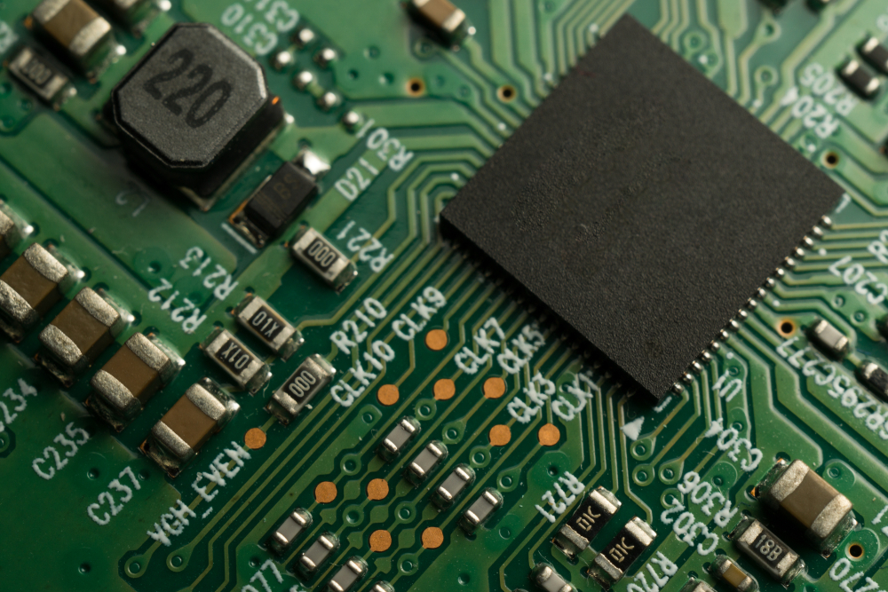
The principle of RF circuit layout is that the RF signal is as short as possible, and the input is far away from the output. The RF circuit is best arranged in a line, and secondly, it can be arranged in an L-shaped arrangement, or it can be arranged at an obtuse angle greater than 90 degrees (such as an angle of 135 degrees). There is also a U-shaped layout, which mainly depends on the space and wiring needs. The U-shaped layout is used when conditions are really limited, and the distance between two parallel lines is controlled to be at least 2mm. Highly sensitive devices such as filters need to add a metal shield, and the place where the microstrip line enters and exits the shield must be slotted. RF area and other areas (such as voltage stabilizing block area, numerical control area) should be arranged separately; high-power amplifiers, low-noise amplifiers, frequency synthesizers, etc. need to be arranged separately, and they should be separated by barriers.
2 About impedance
Factors related to impedance are line width, thickness of dielectric plate, dielectric constant of dielectric plate, copper thickness and so on. In the radio frequency, 50 ohms is often used as the impedance matching standard. The material of the radio frequency dielectric board is usually Rogers series board, such as Rogers 4350 material. Assuming we choose 0.254mm thickness, then according to the simulation, the line width is 0.55mm and the copper thickness is If 0.5OZ is selected, the impedance can be controlled to 50 ohms at this time. For other models, plates of other thicknesses can be simulated based on their dielectric constant and thickness. It is recommended that you use the Polar SI8000 impedance calculation tool for calculation, which is simple and convenient.
3 About the stacked structure
The top layer of the RF board is generally placed with devices and microstrip lines. The second layer needs to be covered with a large area of network copper. The bottom layer should also be a complete ground plane. The copper layer should directly contact the cavity plane. Multi-layer signal line layers are required, so a ground plane should be added between adjacent signal line layers, and the two signal line layers should be routed vertically. Since the board cannot use non-ground network through holes, other networks except ground holes should use blind hole design. If an eight-layer board, in order to effectively use the stack, the seventh layer is preferably a signal line layer, so there will be a large number of 1 Up to 7 blind holes, in actual processing, such a blind hole design will cause serious warpage of the circuit board. The solution is to use a back drill, which is to make the blind hole according to the through hole, and then remove the metallization from the bottom up. Between the hole copper of the hole and the seventh and eighth layers, do not go to the seventh layer. In order to make the performance more stable and eliminate the uncertainty, the hollow part can be filled with resin
4 Matters needing attention in circuit board design
1) The duplexer, mixer and intermediate frequency amplifier always have multiple RF and IF signals interfering with each other, so the interference must be minimized. RF and IF traces should be crossed as much as possible, and a piece of grounding copper should be placed between them as much as possible, and more grounding vias should be made.
2) Place as few non-ground vias as possible within 2 times the line width of the microstrip line of the RF board, and the size of the vias should be as small as possible, which can not only reduce the path inductance, so that the copper paving of the main ground plane will be as complete as possible and placed The RF signal energy is passed through the vias, causing leakage
3) The microstrip line of the radio frequency board should be windowed, that is, no green oil solder mask. The actual measurement shows that it has an improvement effect on the performance of the radio frequency circuit PCB.
4) A row of ground holes should be placed on the edge of the radio frequency signal at a distance of 1.5 times the line width parallel to the radio frequency line. This distance should not be too close. The simulation shows that if the ground is too close to the microstrip line, part of the RF energy will be coupled. To the ground, it will cause a certain loss, the ground hole should be small and dense, the diameter is generally 0.2mm to 0.3mm, and the distance is generally 0.6mm to 1mm. This ground hole can suppress the crosstalk between the microstrip lines. In actual wiring, due to Some circuit boards have signal lines in the inner layer, and the lines are intricate, and there are often many places where isolation holes cannot be placed. Then the solution is to change the ground hole that encounters the signal line to 1 to 2 blind holes. The integrity of the ground hole is greatly preserved, and crosstalk is effectively suppressed

5 About hemming
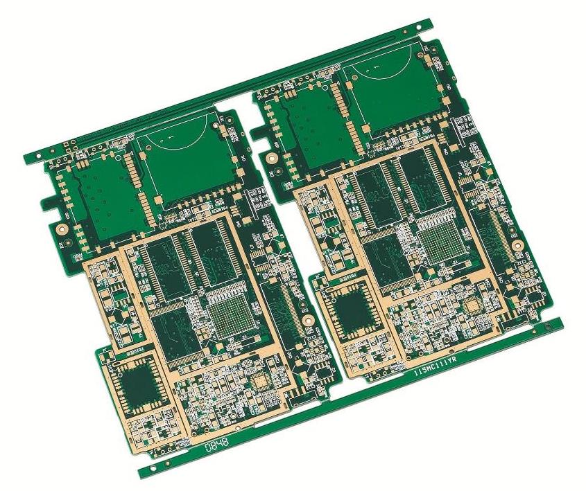
The edging processing of the circuit board, the network metalization edging processing around the radio frequency circuit board can reduce the loss of the radio frequency signal, because the circuit board is made by jigsaw in the actual production process, and the metalization of the board edge is required The shape of the metal-clad edge is cut before the through-hole sinking copper. At this time, the circuit board has not been finished yet, so the board must be connected together by some connecting tapes, so it cannot be cut all. Generally, we These connecting straps will be placed far away from the RF area and as short as possible. Generally, the board manufacturer will require two connecting straps on each side, and not shorter than 5mm. Generally, the microstrip line at the RF input and output must be topped. When it comes to the edge of the board, we will require the board factory to complete the edge at this position. Since the edge is on the same network as the earth, it will be short-circuited with the microstrip line. Then we require our circuit board to return to the process assembly department of our company. After that, use a scalpel to gently scrape it away from the ground network. The reason why we do this is to keep the edging as complete as possible, and the connection belt is far away from the RF zone.
6 About the handling of radio frequency circuit board power
As we all know, the power supply of the circuit needs a decoupling capacitor to filter the power supply to remove interference. RF chips are more sensitive to the power supply. Decoupling capacitors and isolation inductors are needed to filter the noise interference of the power supply. The power supply of the radio frequency circuit should be introduced immediately after the circuit board. Perform filtering and distribute to various parts of the circuit by the voltage regulator block. In order to reduce current loss and generate voltage drop, the power is best passed through the inner layer through the blind hole to the required devices. The power supply of the RF circuit generally does not need to be divided into the plane, and the whole block The power plane will interfere with the RF signal, so it only needs to meet the current requirements to supply power through the inner layer. However, in order to avoid voltage drop, the power line should be as short as possible and not compatible with microstrip. Line overlapping routing, but also to avoid loops. In addition, the decoupling power supply around the chip and the via holes on the grounding pad should be placed as close as possible to the capacitor pad, and the capacitor's grounding pad needs to be laid with a large area of copper. It should be noted here that the aperture and quantity of the vias should be selected according to the current size.
7 About surface treatment
RF boards often require gold wire bonding, which cannot be met by ordinary surface treatment. Conventionally, electroplating thick gold is used, and the gold thickness is controlled above 2um to achieve the adhesion requirements of gold wire bonding. Purity has a lot to do with it. Due to the gold plating process requirements, the pads must be physically connected, so that all pads can be plated with gold by electroplating. This appears between the two pads that should not be connected together in the PCB circuit board we designed. There is a thin process line that needs to be manually removed before the circuit board is soldered. It not only takes time but also destroys the smoothness and integrity of the line. It is not realistic to leave the process line for complex multi-layer boards. In the actual gold plating process, it is generally It is a method of pressing aluminum wire on the copper skin and then electroplating gold to remove the aluminum wire after gold plating. The disadvantage of this is that the aluminum wire pressing point cannot be plated with gold. The electroless nickel-palladium-gold process has proven to achieve a perfect bonding effect and does not require a process line. It can be achieved by controlling the thickness of metal nickel, palladium, and gold. Nickel generally does not need special control according to the conventional thickness. The thickness is generally controlled at 3 microinches.