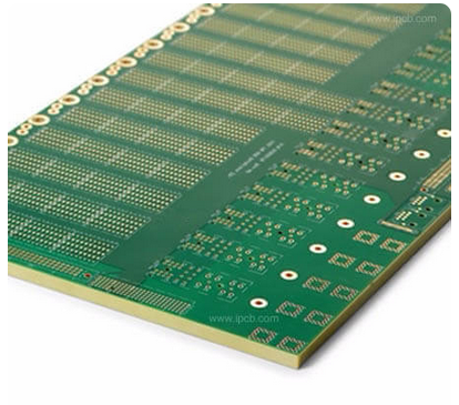
Most thin-film passive devices in RF/Microwave circuit board are also based on the multilayer ceramic firing technique, in which multiple layers of highly conductive metal alloy electrode layers and low-loss ceramic insulation layers are staggered to obtain the required capacitance values. The resultant lamination is then fired at high temperatures to form a monolithic structure. This process still meets the needs of the large capacity of capacitors and high power capacitors very well.
However, the multilayer ceramic process may result in differences between batches and between products in the same batch in certain parameters that are important to the RF designer, such as Q values, ESR, changes in insulation resistance, and changes in capacitance values over a specified tolerance range. Although there are many applications in which these parameter variations do not have a negative impact, current technological breakthroughs in the field of thin-film element production are providing designers with an alternative to producing high-frequency microwave board elements.

The same thin-film technology used to produce semiconductors can also be used to produce thin-film passive components with strict electrical and physical properties. The wire width and insulation layer thickness can be up to 1μm and 10nm respectively.Strict linewidth sizes lead to strict parameter tolerances (inductance values and capacitance values), and several other electrical performance advantages can be further optimized. Due to the high vacuum electrode deposition process, the ESR values are extremely stable between product batches and between different products in the same batch. The ultra-pure and low K insulating layer obtained by the chemical vapor deposition (CVD) process makes the Q and ESR values very stable. Impedance values are stable and predictable over a wide frequency range. The flat grid array (LGA) packaging process enables it to reduce parasitic parameters.
These performance advantages of thin-film elements have an impact on design. Often, the number of components required to achieve a particular circuit function can be reduced. By reducing the number of components used, not only will the design size be reduced, but also the assembly time and cost will be saved, and the reliability of the product will be improved. In addition, the overall electrical performance of products using this component will be improved due to its more stable electrical performance and lower loss.
In a typical application, narrow-band notch filters are used to attenuate the accidental differential frequencies and harmonics generated by complex, wide-range, multi-band radio receivers. Due to the near-perfect nature of the film, it is possible to replace the six components used in the double T design with a single high-quality film capacitor.
A thin-film capacitor (shown in Figure 1) also has an unmentioned performance advantage: it responds to only one resonant point because the device is packaged as a multilayer ceramic capacitor (MLCC) using a single insulating layer design. Figure 2 shows a partial S21 forward transmission loss characteristic curve for this film capacitor.

FIG. 1 Structure of film capacitor

FIG. 2 Forward transmission loss characteristic curve of S21
By choosing film capacitor components, PCB manufacturer can obtain the superior electrical performance of single-layer capacitors and enjoy the advantages of MLCC type components. Figure 3 shows the influence of the stability of the performance of the film capacitor on the thickness of the electrode and oxide layer, and the influence of its quality on the K value of the insulating layer.

FIG. 3 The frequency response of the film capacitor has excellent repeatability
We must realize that the use of film capacitors as band-stop filters has limitations. Because film capacitors typically provide only small capacitance values, they are limited to relatively high-frequency band-stop filter designs. If low-frequency designs are involved, an alternative filter method must be used, usually using high Q multilayer RF/microwave circuit board capacitors.
Film inductance.
Film inductors have many practical advantages over air-core inductors (although they do not achieve the same Q). During surface mount, film inductors are easier to grab and place than air-core inductors. It is also convenient to use IR, vapor phase method, and wave process commonly used in assembly. In addition, film inductors can maintain their inductance values during these processes, as well as in handling and strong vibration environments. Although they cannot be tuned in the circuit as air-core inductors can be, once the exact inductance values needed to implement certain circuit functions are determined, thin-film inductors can be used in place of air-core inductors (assuming that the Q value is sufficient).
As in the case of film capacitors, the ESR and loss of the film inductor are significantly reduced due to the line width control and the quality/accuracy of the insulation layer deposition. This allows the finished size to be reduced to the 0402 packages and enables almost any required inductance value to be achieved while tolerating a precision close to 0.05nH. In addition, the stable metallization process enables the film inductor to have high current carrying capacity: the current carrying capacity varies from product to product, up to 1000mA.
Thin-film inductors can be used for frequency compensation of broadband amplifiers. Previously, a resistor/inductor combination was used. As in the case of thin-film capacitors, the use of thin-film inductors can reduce the number of components used in the circuit, thus reducing the finished size, reducing weight, simplifying assembly, reducing costs, and improving reliability.Like film capacitors, film inductors can only provide small inductance values, so their applications are limited.
That said, thin-film inductors can provide designers with a good solution at very high frequencies. A common application example is oscillators with frequencies up to several gigahertz. At high frequencies, it is impractical to use wire-wound inductors because the technology to produce wire-wound inductors with such small inductance values is not available. In this type of application, designers have only two options: use a snake-lined PCB circuit boarddesign to obtain a low inductance value, or choose a miniature surface encapsulated film inductor.