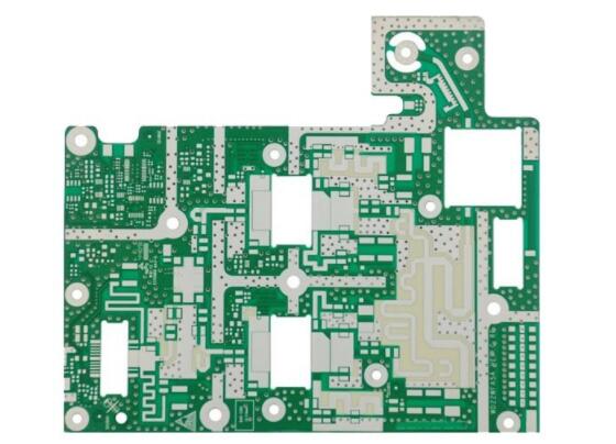
In high-frequency PCB design, engineers need to consider four aspects of interference: power supply noise, transmission line interference, coupling, electromagnetic interference (EMI).
1., Power supply noise
In the high-frequency circuit board, the noise of the power supply has an obvious influence on the high-frequency signal. Therefore, the first requirement of the power supply is low noise. A clean floor is as important as a clean power supply. The power supply has a certain impedance, and the impedance is distributed throughout the power supply. Therefore, the noise will also be superimposed on the power supply. Then we should minimize the impedance of the power supply, so it is best to have a dedicated power supply layer and grounding layer. In hf circuit design, it is much better to design the power supply as a layer than as a bus in most cases, so that the loop can always follow the path of minimal impedance. In addition, the power board must provide a signal loop for all generated and received signals on the PCB. This minimizes the signal loop and thus reduces noise, which is often overlooked by low-frequency circuit designers.

There are several ways to eliminate power noise in PCB design:
1. Pay attention to the through-hole on the board: the through-hole makes the power supply layer need to etch the opening to leave space for the through-hole through. If the opening of the power supply layer is too large, it is bound to affect the signal loop, the signal is forced to bypass, the loop area increases, and the noise increases. At the same time, if several signal lines are clustered near the opening and share the same loop, the common impedance will cause crosstalk.
2, the connection line needs enough ground: each signal needs to have its proprietary signal loop, and the loop area of the signal and loop is as small as possible, that is to say, the signal and loop should be parallel.
3, analog and digital power supply to separate: high-frequency devices are generally very sensitive to digital noise, so the two should be separated, connected at the entrance of the power supply, if the signal across the analog and digital parts of the words, you can place a loop across the signal to reduce the loop area. The digital-analog span used for the signal loop is shown in Figure 3.
4. Avoid overlapping of separate power supplies between different layers: otherwise, circuit noise can easily pass through parasitic capacitive coupling.
5, isolation of sensitive components: such as PLL.
6. Place the power line: to reduce the signal loop, place the power line on the edge of the signal line to reduce the noise.
2, Transmission line
There are only two transmission lines in PCB: ribbon line and microwave line. The biggest problem of the transmission line is reflection, which will cause many problems. For example, the load signal will be the superposition of the original signal and the echo signal, which will increase the difficulty of signal analysis. Reflection causes return loss (return loss), which affects the signal as badly as additive noise interference:
(1) The signal reflected to the signal source will increase the noise of the system, making it more difficult for the receiver to distinguish noise from the signal;
(2) Any reflected signal will reduce the signal quality, will change the shape of the input signal. Generally speaking, the solution is mainly impedance matching (for example, the impedance of the interconnection should very match the impedance of the system), but sometimes the calculation of impedance is more troublesome, you can refer to some transmission line impedance calculation software.
The methods of eliminating transmission line interference in PCB design are as follows:
(a) Avoid impedance discontinuity of transmission lines. The point of discontinuous impedance is the point of transmission line mutation, such as a straight corner, through-hole, etc., should be avoided as far as possible. Methods: To avoid straight corners of the line, as far as possible to go 45° Angle or arc, large Angle can also be; Use as few through-holes as possible, because each through-hole is an impedance discontinuity, and the outer signal avoids passing through the inner layer and vice versa.
(b) Do not use stake lines. Because any pile line is a source of the noise. If the pile line is short, it can be connected at the end of the transmission line; If the pile line is long, it will take the main transmission line as the source and produce great reflection, which will complicate the problem. It is recommended not to use it.
3, coupling
(1) Common impedance coupling: it is a common coupling channel, that is, the interference source and the interfered device often share some conductors (such as loop power supply, bus, public grounding, etc.). In this channel, the drop back of the Ic causes a common-mode voltage in the series current loop, affecting the receiver.
(2) The field common-mode coupling will cause the radiation source to cause common-mode voltage in the loop formed by the interfered circuit and on the common reference surface. If the magnetic field is dominant, the value of the common-mode voltage generated in the series ground circuit is Vcm=-(△B/△t)* area (where △B= change in magnetic induction intensity). If it is an electromagnetic field when its electric field value is known, its induced voltage: Vcm=(L* H *F*E)/48, the formula is suitable for L(m)=150MHz, beyond this limit, the calculation of the maximum induced voltage can be simplified as Vcm=2* H *E.
(3) Differential mode field coupling: refers to the direct radiation is induced and received by the wire pair or the lead on the circuit board and its loop. If you get as close to the two wires as possible. This coupling is greatly reduced, so the two wires can be twisted together to reduce interference.
(4) inter-line coupling (crosstalk) can make any line equal to the parallel circuit between unwanted coupling, serious will greatly damage the performance of the system. Its type can be divided into capacitive crosstalk and perceptual crosstalk. The former is because the parasitic capacitance between the lines makes the noise on the noise source coupled to the noise receiving line through current injection. The latter can be thought of as the coupling of signals between the primary stages of an unwanted parasitic transformer. The size of inductive crosstalk depends on the proximity of the two loops, the size of the loop area, and the impedance of the load affected.
(5) Power line coupling: it refers to the transmission of electromagnetic interference to other equipment after the AC or DC power line is interfered with.
There are several ways to eliminate crosstalk in PCB design:
1. The size of the two kinds of crosstalk increases with the increase of load impedance, so the signal line sensitive to interference caused by crosstalk should be properly terminated.
2, as far as possible to increase the distance between signal lines, can effectively reduce capacitive crosstalk. Ground management, spacing between wiring (such as active signal lines and ground lines for isolation, especially in the state of the jump between the signal line and ground to interval) and reduce lead inductance.
3. Capacitive crosstalk can also be effectively reduced by inserting a ground wire between adjacent signal lines, which must be connected to the formation every quarter wavelength.
4. For sensible crosstalk, the loop area should be minimized and, if allowed, the loop eliminated.
5. Avoid signal sharing loop.
6, pay attention to signal integrity: the designer should realize the end connection in the welding process to solve the signal integrity. Designers using this approach can focus on the microstrip length of the shielding copper foil to obtain a good performance of signal integrity. For systems with dense connectors in the communication structure, the designer can use a PCB as the terminal.
4., Electromagnetic interference
As the speed increases, EMI becomes more and more serious and presents in many aspects (such as electromagnetic interference at interconnects). High-speed devices are particularly sensitive to this and will receive high-speed spurious signals, while low-speed devices will ignore such spurious signals.
There are several ways to eliminate electromagnetic interference in PCB design:
1. Reduce loops: Each loop is equivalent to an antenna, so we need to minimize the number of loops, the area of loops, and the antenna effect of loops. Make sure the signal has only one loop path at any two points, avoid artificial loops, and use the power layer whenever possible.
2, filtering: in the power line and the signal line can take filtering to reduce EMI, there are three methods: decoupling capacitor, EMI filter, magnetic components.
3, shielding. As a result of the length of the issue plus a lot of discussion shielding articles, no longer a specific introduction.
4, try to reduce the speed of high-frequency devices.
5, increase the dielectric constant of the PCB board, can prevent high-frequency parts such as transmission line near the board from radiating outward; Increase the thickness of PCB board, minimize the thickness of microstrip line, can prevent electromagnetic line spillover, can also prevent radiation.