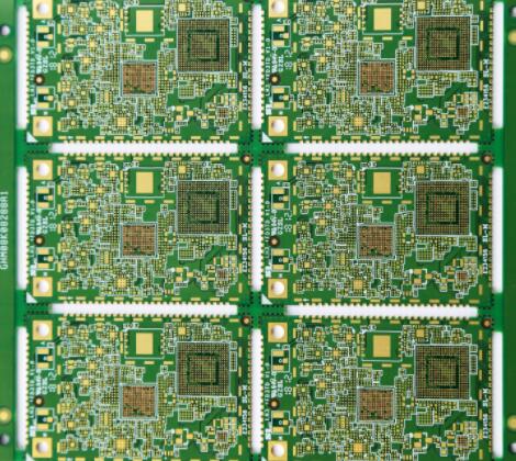
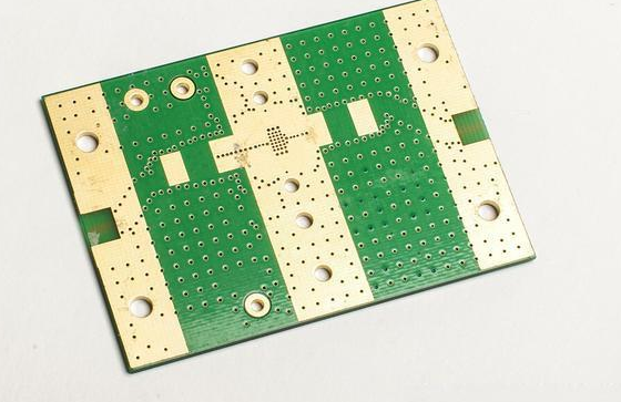
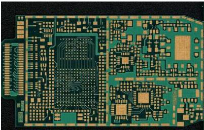
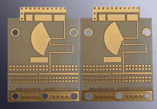
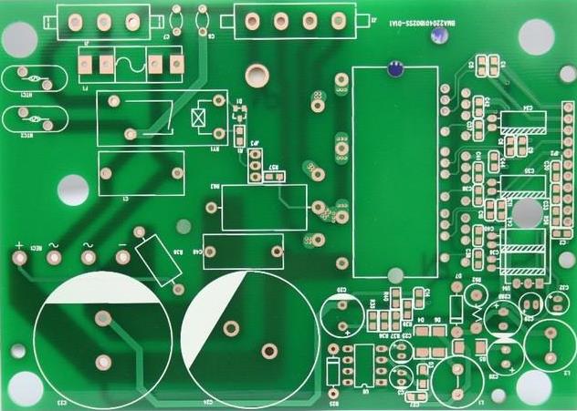
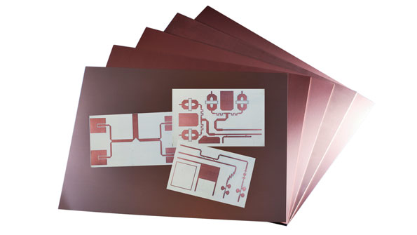
The printed circuit board can form industrialization, large-scale production, the most important is due to some well-known international companies in the 1960s launched about chemical copper plating patent formula and colloidal palladium patent formula. The adoption of electroless copper plating through-holes of printed circuit boards has laid a good foundation for its industrialization, large-scale production, and automatic production. It has also become one of the basic processes for the manufacture of printed circuit boards accepted by various manufacturers. Next, the electroplating process of the circuit board is briefly introduced.
(1) Graphic electroplating method
Copper clad foil plate - drilling - deburring - surface cleaning - weak corrosion - activation - chemical copper plating - whole plate copper plating - etching electroplating graphic image - graphic electroplating copper-tin plating lead or nickel gold - removing resist - etching - hot melt - coating resistance layer.
(2) whole plate plating method
Copper clad foil plate - drilling - deburring - surface cleaning - weak corrosion - activation - electroless copper plating - full plate copper plating - film or screen printing - etch - retreat resist - solder resistance - hot air leveling or electroless nickel gold plating.

The above printed circuit board manufacturing process has a chemical copper plating process, chemical copper plating is a very important link in the printed circuit board manufacturing process. The characteristic of electroless copper plating is that the solution contains a complexing agent or chelating agent. Its reducing agent is formaldehyde.
Complexing agents and formaldehyde in electroless copper plating solution will harm the environment, and it is very difficult to treat wastewater. In addition, the maintenance and management of electroless copper baths are also difficult. However, electroless copper plating is still an important process in the manufacture of the printed circuit board.
The precise technology required by electronic products and the strict requirements of environmental and safety adaptability has prompted the practice of electroplating to make great progress, which is reflected in the manufacturing of high complexity, high-resolution multi-substrate technology. In electroplating, electroplating technology has reached a high level through the development of automated, computer-controlled electroplating equipment, the development of highly sophisticated instrumentation techniques for chemical analysis of organics and metal additives, and the emergence of techniques for precise control of chemical reaction processes.
There are two standard methods for metal growth in circuit board conductors and through holes: line plating and full plate copper plating, described below.
1. Line plating
The process accepts copper layer generation and etching inhibitor metal plating only where the circuit pattern and through-hole are designed. During the line plating process, the width of the line and pad on each side increases roughly as much as the thickness of the electroplated surface, so a margin needs to be left on the original film.
Inline electroplating most of the copper surface should be shielded by a blocking agent, and only electroplating is carried out where there are circuit graphics such as lines and welding pads. Due to the reduced surface area to be electroplated, the required power current capacity is usually greatly reduced. In addition, when using contrast reversal photosensitive polymer dry film electroplating resists (the most commonly used type), the negative film can be produced using a relatively inexpensive laser printer or drawing pen. Less copper is consumed by the anode in line electroplating, and less copper needs to be removed during etching, thus reducing the analysis and maintenance costs of the electrolytic cell. The disadvantage of this technique is that the circuit pattern needs to be coated with tin/lead or an electrophoretic inhibitor material before etching, which can be removed before applying welding inhibitors. This adds to the complexity by adding a set of wet chemical solution treatment processes.
2. Whole plate copper plating
In this process all surface areas and drilling are copper plated, some inhibitor is poured on the unwanted copper surface, and then etching inhibitor metal is plated. Even for a medium-sized printed circuit board, this requires a fairly large current supply to produce a smooth, bright copper surface that is easy to clean for subsequent use. If a photoplotter is not available, negative film is used to expose circuit graphics, making it a more common contrast reversal dry film photoresist. When etching a full copper-plated circuit board, most of the material on the circuit board will be removed again due to the etch agent.With the increase of medium copper carriers, the additional corrosion burden of the anode is greatly increased.
For the manufacture of printed circuit boards, line plating is a better method, its standard thickness is as follows:
1) copper
2) Tin-lead (wiring, welding pad, through-hole)
3) nickel 0.2 mil
4) Gold (connector top) 50μm
These parameters are maintained in the electroplating process to provide the metal plating with high electrical conductivity, good weldability, high mechanical strength, and ductility required to withstand the component terminal panels and copper filling from the PCB board surface to the plating through holes.