1., the introduction
With the gradual increase of PCB board design complexity, the analysis of signal integrity in addition to reflection, crosstalk, and EMI, stable and reliable power supply has become one of the key research directions of designers. Especially when the number of switching devices is increasing and the core voltage is decreasing, the fluctuation of power supply will often bring fatal influence to the system, so people put forward a new term: power integrity, PI (power integrity). In today's international market, IC design is more developed, but the power integrity design is still a weak link. Therefore, this paper puts forward the generation of power supply integrity problem in PCB board, analyzes the factors affecting power supply integrity, and puts forward the optimization method and experience design to solve the power supply integrity problem in PCB board, which has strong theoretical analysis and practical engineering application value.

2, the cause and analysis of power supply noise
The source of power noise is analyzed by a NAND gate circuit diagram. The circuit diagram shows the structure of a three-input Nand gate. Since the NAND gate is a digital device, it works by switching between "1" and "0" levels. With the continuous improvement of IC technology, the switching speed of digital devices is faster and faster, which introduces more high-frequency components, and the inductance in the loop is easy to cause the fluctuation of power supply at high frequency. As shown in Figure 1, when the input of the NAND gate is all at high voltage, the triode in the circuit turns on, the circuit shorts instantly, and the power supply charges the capacitor and flows into the ground wire at the same time. At this time, because of the parasitic inductance on the power line and ground wire, we know from the formula V=LdI/dt that this will generate voltage fluctuations on the power line and ground wire, and the δ I noise introduced by the level rising edge as shown in Figure 2. When the input of the Nand gate is at a low current level, the capacitor discharges at this time, and large δ I noise will be generated on the ground wire. At this time, the power supply only has the current mutation caused by the instantaneous short circuit of the circuit, because there is no charge to the capacitor, the current mutation is smaller than the rising edge. From the analysis of the circuit of NAND gate, we know that the source of power supply instability mainly lies in two aspects: one is the device high-speed switching state, the transient alternating current is too large.

The second is the inductance existing in the current loop. The so-called ground power integrity problem refers to that in high-speed PCB when a large number of chips are on or off at the same time, large transient current will be generated in the circuit, and the voltage fluctuation will be generated on both the power line and the ground line due to the existence of inductance resistance. Understanding the nature of the power supply integrity problem, we know that to solve the power supply integrity problem, first of all, for high-speed devices, we add a decoupling capacitor to remove its high-frequency noise component, to reduce the transient time of the signal; For the inductance existing in the loop, we have to consider the layered design of the power supply.
3, the application of decoupling capacitor
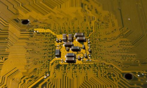
Decoupling capacitors play an important role in high-speed PCB design, and their placement is also very important. This is because when the power supply supplies power to the load for a short time, the storage charge in the capacitor can prevent the voltage drop, such as improper capacitor placement can make the line impedance is too large, affecting the power supply. At the same time, the capacitor can filter the high-frequency noise during the high-speed switching of the device. In high-speed PCB design, we generally add a decoupling capacitor at the output end of the power supply and the input end of the power supply of the chip respectively. The capacitance value near the power supply is generally larger (such as 10μF). This is because the DC power supply is generally used in PCB, and the resonant frequency of the capacitor can be relatively low to filter the noise of the power supply. At the same time, large capacitance can ensure the stability of the power supply output. For the chip connected to the power supply of the pin location of the decoupling capacitor, its capacitance value is generally small (such as 0.1μF), this is because, in high-speed chips, noise frequency is generally relatively high, which requires the added decoupling capacitor resonance frequency to be high, that is, the capacity of the decoupling capacitor to be small.
As for the placement of the decoupling capacitor, we know that improper position will increase the line impedance, reduce its resonant frequency and affect the power supply. For the decoupling capacitor and the inductance in the chip or power supply, we can calculate by the formula. L: the line length between the capacitor and the chip; R: line radius; D: distance between power line and ground.Thus, we know that to reduce inductance L, L and D must be reduced, that is, the loop area formed by decoupling capacitor and chip should be reduced, that is, capacitance and chip should be as close to the chip device as possible.
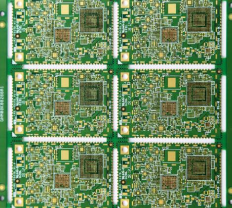
4., the design of the power loop
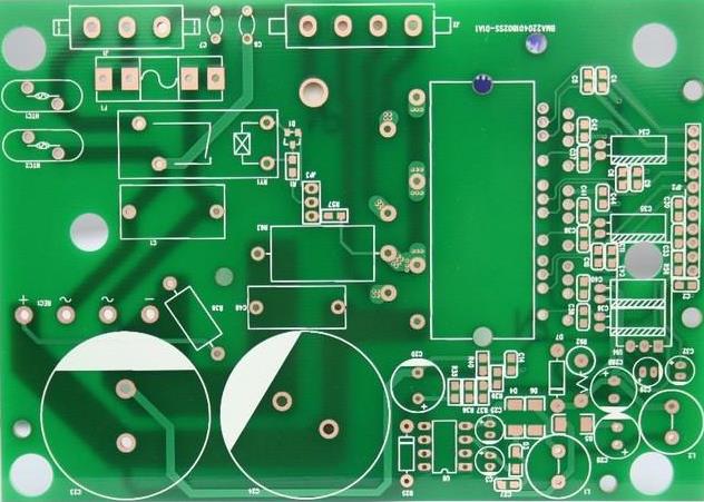
To ensure power supply integrity, we know that a good power distribution network is essential. First of all, for the design of the power line and ground wire, we should ensure that the line width is thick (such as 40mil, while the ordinary signal line is 10mil), to reduce its impedance value as much as possible. As chips get faster and faster, according to the 5/5 rule, we are increasingly using multilayer board, which are powered by a dedicated power layer and circuited by a dedicated layer, thus reducing the inductance of the line.