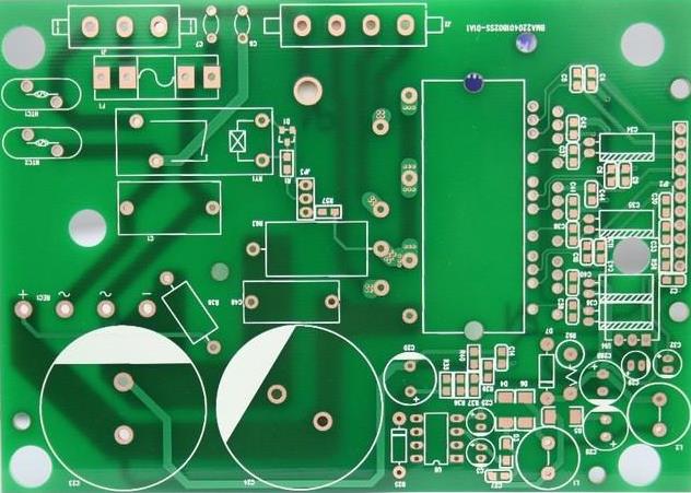
1., PCB board surface treatment
Oxidation resistance, tin spraying, lead-free tin spraying, gold sinking, tin sinking, silver sinking, hard gold plating, whole plate gold plating, gold finger, nickel palladium OSP: lower cost, good solderability, harsh storage conditions, short time, environmental protection process, good welding, smooth.
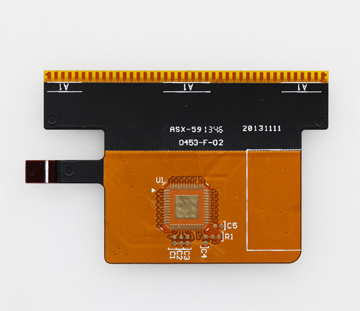
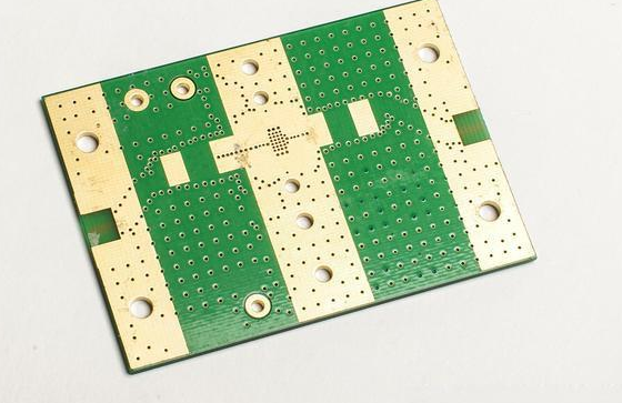
Tin: Tinjet board is usually a multi-layer (4-46 layer) high-precision PCB sample, which has been used by many large communication, computer, medical equipment, and aerospace enterprises and research units in China. The gold finger is made up of many golden conductive contacts, which are gold-plated and arranged in a finger-like manner. Gold fingers are coated with a special layer of gold on top of copper-clad plates because gold is highly resistant to oxidation and highly conductive. Because the price of gold is expensive, however, the current tin plating is used to replace the more memory, tin material from the last century 90 s began to spread, the motherboard, memory, and video devices such as "golden finger" is almost always used in the material, only some high-performance server/workstation accessories will contact point to continue the practice of using gold plated, the price expensive.

2, Why use a gold plate?
With the higher degree of integration of IC, IC feet are denser. The vertical tin-spraying process is difficult to flatten the thin pad, which brings difficulties to SMT. In addition, the shelf life of tin-sprayed plates is very short. And the gold plate is a good solution to these problems:
1, for the surface mount process, especially for 0603 and 0402 ultra-small table paste, because the flatness of the pad is directly related to the quality of the paste printing process, the reflow welding quality has a decisive impact on the back, so the whole plate gold plating is often seen in the high-density and ultra-small table paste process.
2. In the trial production stage, affected by factors such as component procurement, it is often not to weld the plates immediately after they come, but to wait for several weeks or even one month before they are used. The shelf life of gilded plates is many times longer than that of a lead-tin alloy, so everyone is willing to adopt them. Moreover, the cost of gold-plated PCB in the sample stage is almost the same as that of a lead-tin alloy plate.
However, as the wiring becomes denser, the line width and spacing have reached 3-4mil.
Therefore, the problem of short circuit of gold wire is brought: with the increasing frequency of the signal, the effect of signal transmission in the multi-coating caused by skin effect on the signal quality is more obvious.
Skin effect refers to high-frequency alternating current, current will tend to concentrate on the surface of the wire flow. According to the calculation, the skin depth is related to frequency.
3, Why use a sunken gold plate?
To solve the above problems of the gold-plated plate, the PCB with gold-plated plate has the following characteristics:
1, because the crystal structure formed by sunken gold and gold plating is not the same, sunken gold will be golden yellow more yellow than gold plating, customers are more satisfied.
2. Because of the different crystal structures formed by sunken gold and gold plating, sunken gold is easier to weld than gold plating, which will not cause poor welding and cause customer complaints.
3. Because there is only nickel gold on the pad of the gold-plated plate, the signal transmission in the skin effect is in the copper layer, which will not affect the signal.
4. Because the crystal structure of sunk gold is more compact than that of gold-plated gold, it is not easy to produce oxidation.
5, because the gold plate only has nickel gold on the pad, so it will not produce gold wire resulting in slightly short.
6, because the gold plate only has nickel gold on the pad, so the combination of resistance welding and copper layer on the line is more solid.
7, the project will not affect the spacing when making compensation.
8, because the crystal structure formed by gold and gold plating is not the same, the stress of the gold plate is easier to control, which is more conducive to the processing of the state. At the same time, because the gold is softer than gold, so the gold plate is not wear-resistant.
9. The smoothness and service life of the sunken gold plate is as good as that of the gold-plated plate.
4., Sunken gold plate VS gold plate
The gold-plating process is divided into two kinds: one is electroplated, one is sunk gold. For the gold-plating process, the effect of tin is greatly reduced, and the tin effect of gold is better; Unless the manufacturer is required to bind, now most of the manufacturers will choose to sink the gold process! In general, the surface treatment of PCB is as follows: gold-plated (electroplated, gold-immersed), silver plated, OSP, tin-spraying (lead and lead-free), which is mainly for FR-4 or CEM-3 plate, paper base material and rosin coated surface treatment; On tin bad (tin eating bad) this if the exclusion of solder paste and other patch manufacturers production and material technology reasons.
Here only for PCB problems, there are several reasons:
1. In PCB printing, whether there is an oil permeable film surface on PAN position, which can block the effect of tin coating; This can be verified by a tin-bleaching test.
2. Whether the pan position meets the design requirements, that is, whether the design of the pad can be enough to ensure the support of parts.
3. The pad is not contaminated, which can be obtained by ion pollution test; The above three points are the key aspects considered by PCB manufacturer.
The advantages and disadvantages of several ways of surface treatment are each have their strengths and weaknesses! Gold-plating, it can make The PCB storage time is longer, and by the external environment temperature and humidity change is small (relative to other surface treatment), generally can be saved for about a year. Tin spray surface treatment, OSP again, these two kinds of surface treatment in the environment temperature and humidity storage time to pay attention to many.