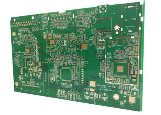
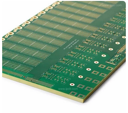
In the circuit board surface treatment, there is a very common use of the process, called gold. The purpose of the gold sinking process is to deposit nickel gold coating with stable color, good brightness, smooth coating, and good solderability on the printed circuit surface of the PCB board.In simple terms, gold deposition is the use of the chemical deposition method, through a chemical REDOX reaction on the surface of the circuit board to produce a layer of metal coating.
1., The role of the gold sinking process
Circuit board copper is mainly copper, copper solder easily oxidized in the air, it will cause solder bad or poor contact, electrical conductivity, that is, reducing the performance of the circuit board, then need to surface treatment of copper solder, heavy gold is gold plated, gold can effectively cut off copper metal-air and prevent oxidation, Therefore, gold precipitation is a treatment method for surface oxidation prevention. It covers the surface of copper with a layer of gold through a chemical reaction, which is also called gold mineralization.

2, Sunken gold can improve the surface treatment of PCB board
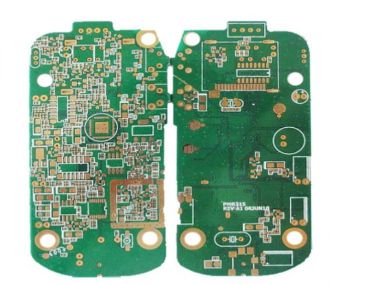
The advantage of the gold sinking process is that the color deposition on the surface of the printed circuit is very stable, the brightness is very good, the coating is very smooth, and the weldability is very good. The thickness of gold, in general, is 1-3 Uinch, so the thickness of gold in this kind of surface treatment is generally thicker, so this kind of surface treatment is widely used in the button board, gold fingerboard, and other circuit boards, because of the strong electrical conductivity of gold, good oxidation resistance, long service life.
3, The benefits of using the circuit board of sunk gold plate
1, heavy gold plate bright color, good color, good appearance, improve the attraction to customers.
2, the crystal structure formed by the precipitation of gold is easier to weld than other surface treatments, can have better performance, to ensure quality.
3, because the gold plate only has nickel gold on the pad, it will not affect the signal, because the signal transmission in the skin effect is in the copper layer.
4. The metal properties of gold are relatively stable, the crystal structure is more compact, and the oxidation reaction is not easy to occur.
5, because the gold plate only has nickel gold on the pad, so the combination of resistance welding and copper layer on the line is more solid, and it is not easy to cause a micro short circuit.
6, the project in the compensation will not affect the spacing, convenient work.
7. The stress of sunk gold plate is easier to control, and the experience is better when using.
4., The difference between heavy gold and gold fingers
A Goldfinger, let's put it bluntly, is a brass contact or a conductor. In detail, because of the strong oxidation resistance of gold, and the conductivity is also very strong, so in the memory and memory slot connected parts plated with gold, so all signals are transmitted through the gold finger. The name comes from the fact that the gold finger is made up of a large number of yellow conductive contacts with a gold-plated surface and arranged like a finger. The gold finger is commonly referred to as the connection between the memory module and the memory slot. All signals are transmitted through the gold finger. A gold finger consists of several gold-colored conductive contacts, which are coated with a special layer of gold on a coppered plate.
Therefore, the simple distinction is that the gold sink is a surface treatment process of the circuit board, and the gold finger is a component with signal connection and conduction on the PCB printed board. In market practice, Goldfinger is not necessarily gold on the surface.