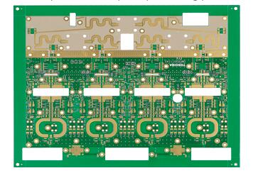
In addition to the impedance of the RF signal line, the laminated structure of the RFPCB high frequency microwave radiofrequency board single board also needs to consider issues such as heat dissipation, current, devices, EMC, structure, and skin effect. Usually, we use multi-layer radio frequency printed boards. Follow some basic principles in layering and stacking:
(1) Each layer of the RFPCB high-frequency microwave radio frequency board is covered with a large area. There is no power plane. The upper and lower adjacent layers of the RF wiring layer should be ground planes.
Even if it is a digital-analog hybrid board, the digital part can have a power plane, but the RF area still has to meet the requirement of large-area paving on each floor.
(2) For the RF double-sided high frequency microwave radio frequency board, the top layer is the signal layer, and the bottom layer is the ground plane.
Four-layer RF high-frequency microwave radio frequency board single board, the top layer is the signal layer, the second and fourth layers are ground planes, and the third layer is for power and control lines. In special cases, some RF signal lines can be used on the third layer. More layers of RF boards, and so on.

(3) For the RF backplane, the upper and lower surface layers are both ground. In order to reduce the impedance discontinuity caused by vias and connectors, the second, third, fourth, and fifth layers use digital signals.
The other stripline layers on the bottom surface are all bottom signal layers. Similarly, the two adjacent layers of the RF high frequency microwave radio frequency board signal layer should be the ground, and each layer should be covered with a large area.
(Iv) For high-power, high-current high-frequency boards, the RF main link should be placed on the top layer and connected with a wider microstrip line.
This is conducive to heat dissipation and energy loss, reducing wire corrosion errors.
(5) The power plane of the digital part should be close to the ground plane and arranged below the ground plane.
In this way, the capacitance between the two metal plates can be used as a smoothing capacitor for the power supply, and at the same time, the ground plane can also shield the radiation current distributed on the power plane.