High frequency PCB design and wiring principles
The principle of high-frequency PCB design and wiring. In the PCB layout stage, a certain amount of printed circuit board size can be properly selected to make full use of the intermediate layer to set up the shield, better achieve near grounding, effectively reduce parasitic inductance, shorten the transmission length and reduce signal crosstalk Etc., all these methods are conducive to the reliability of high-frequency circuits.
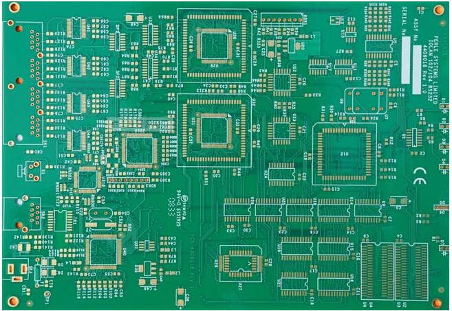
The higher the number of PCB half-layers, the more complicated the manufacturing process and the higher the unit cost. This requires us to select the appropriate number of PCB boards for the PCB layout. Correct component layout planning and correct wiring rules to complete the design. We should also know the layout design principles of these high-speed circuit PCBs: to minimize logic fan-out, it is best to carry only one load. Avoid the use of through holes as much as possible between the output and the receiving end of the high-speed signal line, and avoid the cross of the pin pattern. Especially the clock signal line needs special attention. The signal lines of the upper and lower adjacent layers should be perpendicular to each other to avoid turning at right angles. The parallel termination load resistor should be as close as possible to the receiving end.

Another key area of high-frequency design is the routing of differential pairs, which operate by driving two signal traces in a complementary manner. The differential pair provides excellent noise immunity and a higher S/N ratio. In high-speed PCB design, the control of the characteristic impedance of the circuit board and the design of the topology under multiple loads directly determine the success or failure of the product. The figure shows a daisy-chain topology, which is generally beneficial in the case of a few Mhz. It is recommended to use a star-shaped symmetrical structure on the back end in high-speed PCB design.
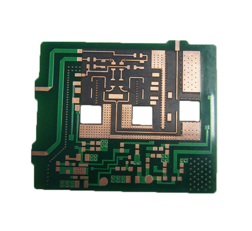
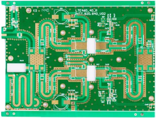
The design of high-frequency circuit PCB is a complicated process, and there are many factors involved, which may be directly related to the working performance of the high-frequency circuit. Therefore, designers need to continuously research and explore in actual work, accumulate experience, and combine with new EDA technology to design high-frequency circuit PCBs with excellent performance.
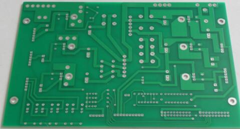
iPCB is a high-tech manufacturing enterprise focusing on the development and production of high-precision PCBs. iPCB is happy to be your business partner. Our business goal is to become the most professional prototyping PCB manufacturer in the world. Mainly focus on microwave high frequency PCB, high frequency mixed pressure, ultra-high multi-layer IC testing, from 1+ to 6+ HDI, Anylayer HDI, IC Substrate,IC test board, rigid flexible PCB, ordinary multi-layer FR4 PCB, etc. Products are widely used in industry 4.0, communications, industrial control, digital, power, computers, automobiles, medical, aerospace, instrumentation, Internet of Things and other fields.