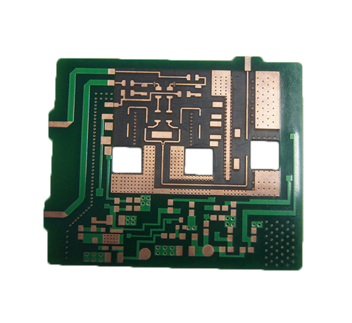
Practical design of PCB board, often see some engineers go line art pursuit, will go get the line on the circuit board horizontal even vertical, looks very beautiful, but some engineers go line is WanWanGuaiGuai, likes to mess the whole, and engineers always pursue short walk the line, can walk sideways line will never cross flat vertical. So is there any difference behind all kinds of wiring styles? This article will introduce the technology and art of PCB wiring.
1. Horizontal and vertical problems
The basic material of PCB is copper-clad board. At present, the common FR-4 is made of electronic glass fiber cloth as reinforcement material, soaked in epoxy resin, covered with copper foil of a certain thickness, and then processed by hot pressing.

At low frequency, the fiberglass cloth has little influence on the electrical properties of PCB, so the medium can be considered as uniform. However, at high frequency, the local characteristics of the dielectric layer will have a great influence on the electrical properties of PCB.
The width and spacing of warp and weft yarns are different for different glass fiber fabrics. If the wiring strategy is horizontal and vertical, the PCB wiring is always 0° or 90° with the edge of the substrate, which will lead to the direction of the transmission line parallel to the warp and weft direction of the glass fiber. At this time, several situations will occur: The transmission line is directly above the meridional glass bundle, the transmission line is directly above the zonal glass bundle, the transmission line is between two meridional glass bundles, the transmission line is between two zonal glass bundles.
Because the relative permittivity of glass fiber cloth is quite different from that of epoxy resin (epoxy resin is about 3, glass fiber cloth is about 6). Therefore, the dielectric constant at different positions of the board surface is different, which leads to the difference of impedance at different positions of the board surface. At the same time, the permittivity of the same impedance line is not uniform due to different positions. The effect on difference pairs is more obvious, which may lead to eye map collapse.
Analysis of the principle of glass fiber effect in PCB
According to the above explanation, horizontal and vertical line although very beautiful, but not necessarily practical, in the actual design, must be functional performance priority, beautiful art second, of course, is both good and good-looking
Problems may not always occur in the actual design, which may depend on the following factors:
Differential wiring is exactly one on the glass fiber bundle, one on the epoxy resin;
The width and length of the line;
The speed of the bus and so on.
2. Solutions
Possible solutions to the above phenomenon are as follows:
Avoid the braided spacing of the glass fiber bundle;
Differential line spacing just avoids the braided spacing of the glass fiber bundle;
Zigzag line;
An angled line;
Designer rotation design;
PCB manufacturer rotating substrate;
Use high-end substrate materials;
Use tighter fiberglass material (fiberglass bundle braided spacing is small);
Electrical upward migration (DESKEW);
Increase electrical allowance and so on.
The above is a brief introduction of the glass fiber effect in PCB. In the actual design process, short physical distance is certainly very important, such as delay, but at the same time, it is necessary to choose a reasonable routing mode according to the difficulty of wiring, transmission line characteristics and so on, and make the design as artistic as possible.