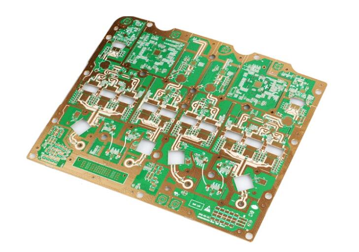
Detailed explanation of PCB high frequency board material and classification
High-frequency board refers to a special circuit board with a higher electromagnetic frequency, used for high-frequency (frequency greater than 300MHZ or wavelength less than 1 meter) and microwave (frequency greater than 3GHZ or wavelength less than 0.1 meter)
The PCB in the category is a circuit board produced by operating the departmental process of the popular rigid circuit board manufacturing method on the microwave substrate copper clad board or adopting a special treatment method. Generally speaking, the high-frequency board can be defined as a circuit board with a frequency above 1GHz.
With the rapid growth of scientific technology, more and more equipment designs are used in the microwave frequency band (>1GHZ) and even in the millimeter wave range (30GHZ). The requirements are getting higher and higher.
For example, the substrate material must have good motor performance, outstanding chemical invariance, and the loss requirement on the substrate with the increase of the frequency of the power signal is very small, so the main nature of the high-frequency sheet is highlighted.
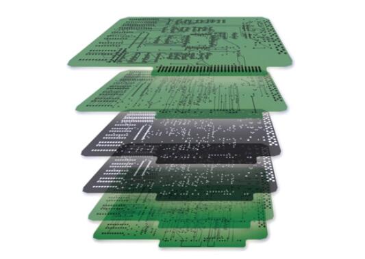
Classification of PCB high-frequency plates 1
Adding thermosetting materials to the end ceramics
Processing methods:
The processing process is similar to epoxy resin/glass woven cloth (FR4), except that the sheet is brittle and easily breaks. When drilling and gongs, the life of the drill tip and gong knife will be reduced by 20%.
2 PTFE (polytetrafluoroethylene) material
Processing method: 1. Cutting material: It is necessary to save the shielding film cutting material to avoid scratches and indentations
2. Drilling:
2.1 Use a brand new drill tip (size 130), one by one is the best, the pressure of the presser foot is 40psi
2.2 The aluminum sheet is the cover plate, and then the 1mm melamine backing plate is used to hold the PTFE plate tightly
2.3 After drilling, use an air gun to blow out the dust in the hole
2.4 Use the most constant drilling rig and drilling parameters (basically, the smaller the hole, the faster the drilling speed, the smaller the Chip load, the lower the return speed)
3 hole disposal
Plasma treatment or sodium naphthalene activation treatment is conducive to hole metallization
4 PTH Immersion Copper
4.1 After micro-etching (with a micro-etching rate of 20 micro inches controlled), start from the de-oil tank and enter the board in the PTH pull
4.2 If necessary, pass the second PTH, just start with the estimated cylinder and enter the board
5 Solder mask
5.1 Pre-treatment: Take acidic washing of the plates, and do not use the machine to grind the plates
5.2 Pre-treatment and post-baking plate (90 degree Celsius, 30min), brush with green oil and solidify
5.3 Three-stage baking: one stage is 80 degree Celsius, 100 degree Celsius, 150 degree Celsius, each for 30 minutes (if the substrate surface is oiled, it can be reworked: wash off the green oil and reactivate it)
6 Gong board
Lay the white paper on the circuit surface of the PTFE board, and clamp the height with the FR-4 substrate board or phenolic bottom plate with a thickness of 1.0MM etched to remove copper:

When selecting the substrate used in the PCB for high-frequency circuits, it is necessary to examine the material DK and its transformation characteristics at different frequencies.
For high-speed signal transmission requirements or characteristic impedance control requirements, the focus is on DF and its performance under the premises of frequency, temperature and humidity.
Under the premise of frequency change of ordinary substrate material, it shows the discipline of greater change in DK and DF values.
Especially in the frequency range from 1 MHz to 1 GHz, their DK and DF values change significantly.
According to the coating online, the DK value of ordinary epoxy resin-glass fiber cloth-based substrate material (ordinary FR-4) at a frequency of 1MHz is 4.
7, and the DK value under the frequency of 1GHz changes to 4.19. Over 1GHz, the change of its DK value tends to be steep.
The trend of its transformation is to follow the increase in frequency, and then become smaller (but the transformation amplitude is not large), for example, under l0GHz, the DK value of ordinary FR-4 is 4.15, and the substrate material with high-speed and high-frequency characteristics changes in frequency. Under the environment, the change of DK value is relatively small. Under the frequency of change from 1MHz to 1GHz, DK is mostly connected to the change of 0.02 scale.
Its DK value tends to drop slightly under the premise of diverging frequency from low to high.
The medium loss factor (DF) of the ordinary substrate material is affected by the frequency change (except for the change in the high-frequency scale) and the change in the DF value is greater than the DK.
Its transformation discipline tends to increase, so when evaluating the high-frequency characteristics of a substrate material, the focus of its examination is its DF value transformation environment.
For substrate materials with high-speed and high-frequency characteristics, there are two different types of common substrate materials in terms of their transformation characteristics at high frequencies: one type changes with frequency, and its (DF) value changes very little. .
Another type is similar to ordinary substrate materials in terms of the transformation amplitude, but its own (DF) value is lower. (PCB factory)