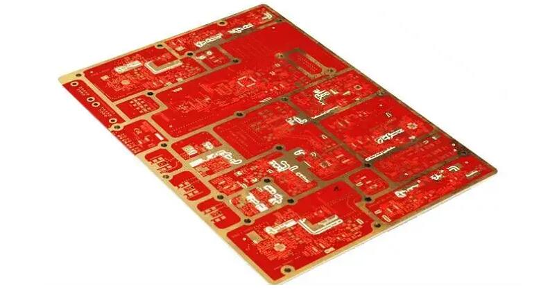
Definition of PCB High Frequency Board
High Frequency Board refers to the special circuit board with high electromagnetic frequency, which is used in the field of high frequency (frequency greater than 300MHz or wavelength less than 1m) and microwave (frequency greater than 3GHz or wavelength less than 0.1M). It is a circuit board produced by using some processes of ordinary rigid circuit board manufacturing method or special treatment method on microwave substrate copper clad laminate. Generally speaking, a high-frequency board can be defined as a circuit board with a frequency above 1GHz.

Classification of PCB High Hrequency Board
1. Ceramic powder filled thermosetting material
Processing method:
The processing process is similar to that of epoxy resin / glass woven fabric (FR4), but the board is brittle and easy to break. When drilling and Gong plate, the service life of drilling nozzle and router knife should be reduced by 20%.

Raw Material
2. PTFE (polytetrafluoroethylene) material
Processing method:
1. Cutting: the protective film must be reserved to prevent scratch and indentation
2. Drilling:
2.1 use new drill nozzles (standard 130), one by one is the best, and the presser foot pressure is 40psi
2.2 the aluminum sheet is the cover plate, and then the PTFE board is tightened with 1mm melamine backing board
2.3 blow out the dust in the hole with an air gun after drilling
2.4 use the most stable drilling rig and drilling parameters (basically, the smaller the hole is, the faster the drilling speed is, and the smaller the chip load is, the smaller the return speed is)
3. Hole treatment
Plasma treatment or sodium naphthalene activation treatment is conducive to pore metallization
4. PTH copper precipitation
4.1 after micro etching (the micro etching rate has been controlled by 20 micro inches), pull the board from the oil cylinder at PTH
4.2 if necessary, pass the second PTH, just from the expected? The cylinder begins to enter the board
5. Resistance welding
5.1 pretreatment: acid board washing shall be adopted instead of mechanical board grinding
5.2 after pretreatment, bake the plate (90 degree Celsius, 30min) and brush it with green oil for curing
5.3 the baking board is divided into three stages: 80 degree Celsius, 100 degree Celsius and 150 degree Celsius for 30 minutes each (if oil is thrown on the substrate surface, it can be reworked: wash off the green oil and reactivate it)
6. Routing board
Lay white paper on PTFE board line pavement and clamp it up and down with FR-4 base board or phenolic base board with thickness of 1.0mm etched and copper removed.
 raw material.jpg")
Raw Material