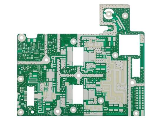
Wiring is a very important part of PCB design, which will directly affect the performance of PCB board. In the process of PCB design, different layout engineers have their own understanding of layout, but all layout engineers are consistent in how to improve the efficiency of wiring, which can not only save the development cycle of the project for customers, but also ensure the quality and cost to the maximum. The following is a general design process and steps.
1. Determine the number of PCB layers
The size of the circuit board and the number of wiring layers need to be determined at the beginning of the design. If the design requires the use of high-density ball grid array (BGA) components, the minimum number of wiring layers required for the wiring of these devices must be considered. The number of wiring layers and stack-up mode will directly affect the wiring and impedance of printed lines. The size of the plate helps determine the layering pattern and the width of the printed line to achieve the desired design effect.
iPCB is committed to providing customers with one-stop online procurement services for electronic components, providing thousands of electronic components procurement, price inquiry and transaction, to ensure that all components are purchased from the original factory or agents through formal channels, to ensure that the original and genuine products, is a professional procurement website for electronic components in China.

2. Design rules and limitations
The automatic routing tool itself does not know what to do. To accomplish the wiring task, the wiring tool needs to work under the correct rules and constraints. Different signal cables have different wiring requirements. The signal cables with special requirements must be classified according to the design. Each signal class should have a priority, and the higher the priority, the stricter the rules. Rules relating to printed line width, maximum number of holes, parallelism, interaction between signal lines, and layer limits have a great impact on the performance of routing tools. Careful consideration of design requirements is an important step in successful wiring.
3. Component layout
To optimize the assembly process, the manufacturability design (DFM) rule imposes restrictions on the layout of components. If the assembly department allows components to move, the circuit can be optimized to facilitate automatic wiring. The rules and constraints defined affect the layout design.
4. Fan out design
During the fan out design phase, to enable the automatic routing tool to connect component pins, each pin of the surface mount device should have at least one through-hole so that the board can be used for inner bonding, in-line testing (ICT), and circuit reprocessing when additional connections are required.
To maximize the efficiency of the automatic wiring tool, it is important to use the largest hole size and printed line possible, with an interval of 50mil being ideal. Use the type of through-hole that maximizes the number of wiring paths. On-line test of circuit should be considered when designing fan out. Test fixtures can be expensive and are usually ordered near full production, when it is too late to consider adding nodes to achieve 100% testability.
5. Manual wiring and key signal processing
Although this paper focuses on automatic wiring, manual wiring is and will be an important process in PCB design. Manual routing is helpful for automatic routing tools. Regardless of the number of critical signals, wiring these signals first, manual wiring or combined with automatic wiring tools. Critical signals usually have to be carefully designed to achieve the desired performance. After wiring is completed, the signal wiring is checked by the relevant engineering personnel, which is a much easier process. After the check is passed, the wires are fixed and automatic wiring of the remaining signals begins.
6. Automatic wiring
Wiring of key signals needs to consider controlling some electrical parameters during wiring, such as reducing distributed inductance and EMC, and wiring of other signals is similar. All EDA vendors provide a way to control these parameters. The quality of automatic wiring can be guaranteed to a certain extent by knowing what input parameters the automatic wiring tool has and how they affect wiring.
7. Circuit board appearance
Previous designs often focused on the visual effects of the circuit board, but that is no longer the case. The circuit board designed automatically is not as beautiful as manual design, but it can meet the requirements of electronic characteristics, and the integrity of the design is guaranteed.
For layout engineers, the technology is strong or not, should not only from the number of layers and speed to judge, only in the number of components, signal speed and other conditions similar to the case, to complete the design of the smaller area, the fewer layers, the lower the cost of the PCB board, and to ensure good performance and beauty, this is the master.