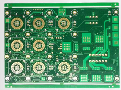
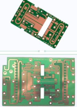
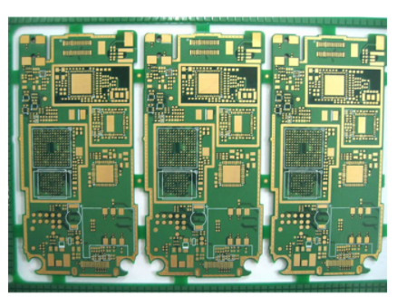
1. How to select PCB board?
Selection of PCB sheets must be balanced between meeting design requirements and scalability and cost. Design requirements include electrical and mechanical components. This material problem is often important when designing very high-speed PCB boards (frequencies greater than GHz).
For example, the dielectric loss of FR-4 materials, which are commonly used today, at several GHz frequencies can have a significant effect on signal attenuation and may not be applicable. For electrical purposes, it is important to note whether dielectric constant and dielectric loss are appropriate at the designed frequency.
2. How to avoid high frequency interference?
The basic idea to avoid high frequency interference is to minimize the interference of high frequency signal electromagnetic field, also known as crosstalk. You can increase the distance between the high-speed signal and the analog signal or add ground guard/shunt traces next to the analog signal. Also note the digital interference to analog ground noise.
3. How to solve the signal integrity problem in high-speed design?
Signal integrity is essentially an impedance matching problem. The factors that affect impedance matching include the structure of the signal source and output impedance, the characteristic impedance of the line, the characteristics of the load side, the topology architecture of the line, and so on. The solution is the termination and the topology of adjusting the route.
4. How is the differential distribution implemented?
There are two points to note in the differential pair wiring: one is that the two lines should be as long as possible, and the other is that the distance between the two lines, which is determined by the differential impedance, should remain constant, that is, parallel. There are two ways of parallel, one is to walk two lines on the same side-by-side, and the other is to walk two lines on the next two levels (over-under). Generally, the former side-by-side (side by side, side by side) implements more ways.
5. How to achieve differential distribution for clock signal lines with only one output?
It is meaningful to use a differential distribution that both the source and the receiver are also differential signals. Therefore, differential distribution cannot be used for clock signals with only one output.
6. Can a matching resistance be added between the differential pairs at the receiving end?
The matching resistance between the differential line pairs at the receiving end is usually added and should be equal to the value of the differential impedance. This will improve the signal quality.
7. Why are the wiring of difference pairs close and parallel?
The wiring of difference pairs should be appropriately close and parallel. The proper proximity is due to the influence of this distance on the value of differential impedance, which is an important parameter in designing differential pairs. Parallel is also required to maintain the consistency of differential impedances. If the two lines are close or far, the differential impedance will be inconsistent, which will affect signal integrity and time delay.
8. How to deal with some theoretical conflicts in the actual wiring
Basically, it is correct to isolate a module/number partition. It is important to note that the signal path should not cross the moat as much as possible, and that the return current path of the power supply and the signal should not become too large.
Crystal oscillation is an analog positive feedback oscillation circuit. In order to have a stable oscillation signal, the specifications of loop gain and phase must be met. The oscillation specifications of analog signals are susceptible to interference, even with ground guard traces, the interference may not be completely isolated. Also, noise on the ground affects the positive feedback oscillator circuit too far away. Therefore, it is important to keep the crystal oscillation close to the chip.
Indeed, there are many conflicts between high-speed cabling and EMI requirements. However, the basic principle is that because of the resistance capacitance or ferrite bead added by EMI, some electrical characteristics of the signal cannot be out of conformity with the specification. Therefore, it is best to use the techniques of routing and PCB overlays first to solve or reduce EMI problems, such as high-speed signals going inside. Finally, the resistance capacitance or ferrite beam is used to reduce the damage to the signal.
9. How to resolve the conflict between manual and automatic wiring for high-speed signals?
Most automatic wiring devices with stronger wiring software now have constraints to control the winding method and the number of holes passed. EDA companies sometimes have very different winding engine capabilities and constraint settings. For example, whether there are sufficient constraints to control the way serpentine snakes snake lines snake, the spacing between differential pairs of lines, and so on.
This will affect whether the way the automatic wiring comes out will match the designer's mind. In addition, the difficulty of manually adjusting the wiring is also absolutely related to the winding engine's ability. For example, the pushing capacity of the line, the pushing capacity of the hole, and even the pushing capacity of the line for copper coating, etc. Therefore, choosing a wiring router with a strong winding engine is the solution.
10. About test coupon.
Test coupon is a TDR (Time Domain Reflectometer) used to measure whether the characteristic impedance of the PCB board produced meets the design requirements. Generally, the impedance to be controlled is a single line and a differential pair. Therefore, the line width and spacing (with differential pairing) on the test coupon should be the same as the line to be controlled.
The most important thing is the position of the ground point when measuring. To reduce the inductance of ground lead, TDR probes are grounded very close to the probe tip, so the distance and manner of the point on test coupon to which the signal is measured should match the probe used.
11. In the design of high-speed PCB, the blank area of the signal layer can be coated with copper, and how should the copper coating of multiple signal layers be distributed on the grounding and power supply?
In general, the vast majority of copper deposits in blank areas are grounded. Only pay attention to the distance between the copper coating and the signal line when copper is applied beside the high speed signal line, because the copper coating will reduce the characteristic impedance of the line a little. Also be careful not to affect the characteristic impedance of its layer, such as when structuring a dual strip line.
12. Can the signal line above the power plane be used to calculate the characteristic impedance using the microstrip line model? Can the signal between the power supply and the ground surface be calculated using the stripline model?
Yes, both the power plane and the ground plane must be considered as the reference plane when calculating the characteristic impedance. For example, four-layer plates: top-power-stratum-bottom, in which case the model of the characteristic impedance of the top line is a microstrip line model with the power plane as the reference plane.
13. Can test points automatically generated by software on high density printed boards generally meet the test requirements of mass production?
Whether test points generated automatically by general software meet the test requirements must depend on whether the specifications for adding test points meet the requirements of the test tool. In addition, if the route is too dense and the specification for adding test points is strict, it may not be possible to automatically add test points to each segment of the line, of course, you need to manually complete where you want to test.
14. Does adding test points affect the quality of high-speed signals?
Whether or not the signal quality will be affected depends on how fast the test point is added and how fast the signal is. Basically additional test points (instead of using via or DIP pins as test points) may be added online or pulled a small segment of line out of the line. The former is equivalent to adding a small capacitor on-line, the latter is a branch.
Both of these conditions will have some influence on how much or how little the high-speed signal is affected, depending on the frequency speed and edge rate of the signal. The size of the impact can be determined by simulation. In principle, the smaller the test point, the better (and of course, to meet the requirements of the test tool) the shorter the branch, the better.
15. Several PCBs form the system. How should the ground wires between the boards be connected?
When the signals or power supply between PCB boards are connected to each other, such as A boards having power supply or signal sent to B boards, there must be an equal amount of current flowing from the ground to A boards (this is Kirchoff current law). Currents in this formation flow back where they have the lowest impedance.
Therefore, the number of pins allocated to the formation at each interface, whether power or signal connected, should not be too small to reduce impedance, which can reduce noise in the formation. In addition, you can analyze the entire current loop, especially the larger part of the current, adjust the connection of strata or ground lines to control the movement of the current (for example, to create a low impedance somewhere so that most of the current moves from this location), and reduce the impact on other more sensitive signals.
16. Can you introduce some foreign technical books and data on high-speed PCB design?
High-speed digital circuits are now used in fields such as communication networks and computers. In terms of communication networks, PCB boards work at frequencies above and below GHz, with as many as 40 layers as I know. Calculator-related applications are also due to advances in chips, such as PCs or servers, where the maximum operating frequency on a board has reached more than 400 MHz (such as Rambus).
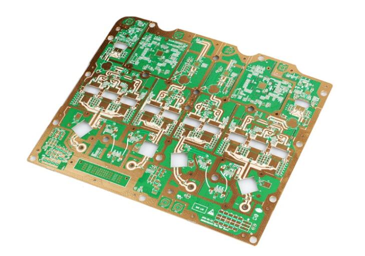
In response to this high-speed and high-density wiring demand, blind/buried vias, mircrovias and build-up process requirements are gradually increasing. These design requirements are manufactured in large quantities by the manufacturer.
17. Two commonly referred characteristic impedance formulas:
Microstrip Z={87/[sqrt(Er+1.41)]}ln[5.98H/(0.8W+T)], where W is the line width, T is the copper skin thickness of the line, H is the distance from the line to the reference plane, and Er is the dielectric constant of the PCB plate material.
This formula must be 0.1<(W/H)<2.0 and 1<(Er)<15 to apply.
Strip line Z=[60/sqrt(Er)]ln{4H/[0.67 pi(T+0.8W)]} where H is the distance between the two reference planes and the line is in the middle of the two reference planes. This formula must be used when W/H < 0.35 and T/H < 0.25.
18. Can a ground line be added between the differential signal lines?
Generally, there is no ground wire in the middle of the differential signal. Because the most important application principle of differential signals is to utilize the benefits of coupling between differential signals, such as flux cancellation and noise immunity. If an intermediate ground line is added, the coupling effect will be destroyed.
19. Does the rigid veneer design require special design software and specifications? Where can I undertake processing of this kind of printed circuit board in China?
Flexible Printed Circuits can be designed with general PCB design software. Also manufactured to FPC vendors in Gerber format. Because the manufacturing process is different from PCBs in general, each manufacturer will have its own ** for minimum line width, minimum line spacing and minimum via according to their manufacturing capability. In addition, the flexible circuit board can be strengthened by laying some copper sheets at the bends. As for the manufacturer, the online "FPC" should be found when the keyword query.
20. What is the principle for properly selecting the point where the PCB is grounded to the housing?
The principle of selecting PCB and shell grounding points is to use chassis groundto provide a path with low impedance to return current and to control this return current. For example, layers of PCB are usually connected to chassis grounds by fixed screws near high frequency devices or clock generators to minimize the area of the entire current loop, which also reduces electromagnetic radiation.
21. From which aspects should DEBUG begin?
As far as digital circuits are concerned, there are three things to decide first:
1. Verify that all power values are up to design requirements. Some systems with multiple power sources may require a specification of the order and speed of the rise of certain power sources.
2. Verify that all clock signal frequencies are working properly and that there is no non-monotonic problem at the edge of the signal.
3. Verify that the reset signal meets the specifications. If this is normal, the chip should signal the first cycle. Next debug according to the operating principle of the system and bus protocol.
22. In the case of fixed circuit board size, if more functions need to be accommodated in the design, it is often necessary to increase the line density of PCB. However, this may lead to increased interference between lines, and too fine lines will prevent the impedance from being reduced. Please refer to experts on techniques in high-speed (>100MHz) high-density PCB design?
When designing high-speed and high-density PCBs, crosstalk interference does require special attention because it has a significant impact on timing and signal integrity. Here are a few things to note:
Controls the continuity and matching of line characteristic impedances.
The size of the line spacing. Twice the line width is usually seen. Simulations can be used to find out the effect of line spacing on time series and signal integrity, and to find the smallest tolerable spacing. The results of different chip signals may be different.
Select the appropriate terminal mode.
Avoid going in the same direction as the adjacent upper and lower layers, or even having lines that overlap up and down exactly, because this kind of crosstalk is greater than that of adjacent upper and lower layers.
Blind/buried via is used to increase line area. However, the cost of PCB board production will increase. It is really difficult to achieve full parallel and equal length in actual execution, but try to do it as much as possible.
In addition, differential and common mode terminals can be reserved to mitigate the effects on timing and signal integrity.
23. Filtering at analog power supply is often done by LC circuit. But why is LC sometimes less effective than RC?
The comparison of LC and RC filters must consider whether the selection of the band and inductance values to be filtered is appropriate. Because the magnitude of the reactance of an inductance is related to the inductance value and frequency. If the noise frequency of the power supply is low and the inductance value is not large enough, the filter effect may not be as good as RC. However, the cost of using RC filter is that the resistance itself consumes energy, is inefficient, and pays attention to the power that the selected resistance can withstand.
24. Inductance is selected for filtering. What is the method of capacitance value?
The selection of inductance value takes into account not only the desired noise frequency, but also the reactivity of instantaneous current. If there is an opportunity for the LC output to output a large current instantaneously, the inductance value is too large to impede the speed at which the large current flows through the inductance and increase ripple noise.
The capacitance value is related to the magnitude of the acceptable ripple noise specification value. The smaller the ripple noise value is required, the larger the capacitance value is. The capacitance ESR/ESL also has an effect. In addition, if the LC is placed at the output of the switching regulation power, pay attention to the effect of pole/zero generated by the LC on the stability of the negative feedback control loop.
25. How to meet EMC requirements as far as possible without causing too much cost pressure?
The cost of EMC on PCB boards is usually caused by increasing the number of strata to enhance the shielding effect and the suppression of high frequency harmonic devices such as ferrite bead and choke. In addition, shielding structures on other institutions are usually required to enable the whole system to pass through EMC requirements. Here are just a few tips for PCB board design to reduce the electromagnetic radiation effect generated by the circuit.
Select devices with a slower signal slope (slew rate) whenever possible to reduce the high frequency component of the signal.
Pay attention to the placement of the high frequency devices and do not go too close to the external connectors.
Note the impedance matching of high-speed signals, the line layer and its return current path to reduce high-frequency reflection and radiation.
Place enough uncoupling capacitance at the power pins of each device to mitigate noise in the power layer and the ground. Particular attention should be paid to whether the frequency response and temperature characteristics of the capacitor meet the design requirements.
The ground near the outer connector can be properly divided with the ground and the ground near the connector can be connected to the chassis ground.
Groundguard/shunt traces can be used appropriately alongside some very high-speed signals. However, it is important to note the effect of guard/shunt traces on the line characteristic impedance.
The power layer is retracted 20H from the formation, and H is the distance between the power layer and the formation.
26. When there are more than one digital/analog function blocks in a PCB board, the general practice is to separate the digital/analog modules. What is the reason?
The reason for the digital/analog separation is that the digital circuit produces noise in the power supply and ground when switching between high and low potentials. The noise level is related to the speed and current of the signal. If the ground level is not divided and the noise generated by the digital area circuit is large and the circuit in the analog area is very close, the analog signal will still be disturbed by the ground noise even if the digital and analog signals do not cross. That is to say, the digital-analog undivided method can only be used when the area of the analog circuit is far from the area of the digital circuit that produces a lot of noise.
27. Another way is to ensure that the digital/analog signals are laid out separately and that the lines of the digital/analog signals do not cross each other, so that the entire PCB floor is not divided and the digital/analog modules are connected to this plane. Why?
The requirement that digital-analog signals cannot cross is that the return current path of a slightly faster digital signal will try to flow back to the source of the digital signal near the bottom of the line. If the digital-analog signals cross, the noise generated by the return current will appear in the area of the analog circuit.
28. How to consider impedance matching in high speed PCB design schematic design?
Impedance matching is one of the key elements in the design of high-speed PCB circuits. However, the impedance value has an absolute relationship with the mode of traveling, such as the distance from the surface layer (microstrip) or the inner layer (stripline/double stripline), the distance from the reference layer (power layer or stratum), the width of the traveling line, the PCB material, etc. all affect the characteristic impedance value of the traveling line. That is to say, the impedance value can only be determined after wiring.
The general simulation software can not take into account some discontinuous impedance distribution due to the line model or the mathematical algorithm used**. At this time, only some terminators, such as series resistors, can be reserved on the schematic diagram to alleviate the effect of the discontinuity of line impedance. The real solution is to avoid impedance discontinuity when wiring.
29. Where can I provide a more accurate IBIS model library?
The accuracy of the IBIS model directly affects the simulation results. Basically, IBIS can be regarded as the data of the electrical characteristics of the actual chip I/O buffer equivalent circuit, which can generally be converted from the SPICE model (also can be measured, but ** is more). The data of SPICE is absolutely related to the chip manufacturing, so the data of SPICE is different from one chip manufacturer to another. The data within the converted IBIS model will then vary.
That is, if manufacturer A's devices are used, only they have the ability to provide accurate model data for their devices, because no one else knows more about what process their devices are made of than they do. If the IBIS provided by a vendor is inaccurate, the only solution is to constantly ask the vendor for improvement.
30. In high-speed PCB design, from which aspects should designers consider the rules of EMC and EMI?
Generally, both radiated and conducted aspects need to be considered in EMI/EMC design. The former belongs to the higher frequency part (>30MHz) and the latter to the lower frequency part (<30MHz). So you can't just focus on the high frequencies and ignore the low frequencies.
A good EMI/EMC design must start with a layout that takes into account the location of the devices, the arrangement of the PCB stacks, the way to go on the important line, the selection of devices, etc. If these are not better arranged beforehand, the solution afterwards will do twice the work and increase the cost.
For example, the position of the clock generator should be as close to the external connector as possible, the high-speed signal should go as far as possible inside and pay attention to the continuity of characteristic impedance matching and reference layer to reduce reflection, the slope of the signal pushed by the device should be as small as possible to reduce the high frequency component, and the decoupling/bypass capacitance should be chosen to reduce the power layer noise.
In addition, note that the return path of the high frequency signal current minimizes the area of the loop (i.e., the loop impedance of the loop) to reduce radiation. It is also possible to control the range of high frequency noise by dividing strata. Finally, choose the appropriate place where the PCB will connect to the shell (chassis ground).
31. How to select EDA tools?
Current PCB design software, thermal analysis is not a strong point, so it is not recommended to select, other functions 1.3. 4 You can choose either PADS or Cadence for a good performance-price ratio. Beginners of PLD design can use the integrated environment provided by the PLD chip manufacturer, and single-point tools can be used when designing over a million doors.
32. Please recommend an EDA software suitable for high speed signal processing and transmission.
In conventional circuit design, the ADS of INNOVEDA is very good and has useful simulation software, which often occupies 70% of the applications. For high-speed circuit design, analog and digital hybrid circuits, the solution using Cadence should be a better performance and price software. Of course, Mentor's performance is still very good, especially its design flow management should be the best. (Wang Sheng, Technical Expert of Datang Telecom)
33. Interpretation of the meaning of each layer of PCB board
Topoverlay - The name of the top device, also known as top silkscreen or top component legend, such as R1 C5,
IC10. Bottomoverlay--The same as multilayer---- If you design a four-layer board, you place a free pad or via and define it as a multilayer, its pad will automatically appear on the four layers, and if you only define it as a top layer, its pad will only appear on the top layer.
What should we pay attention to in the design, wiring and typesetting of high frequency PCB above 34 and 2G?
The high frequency PCB above 2G belongs to RF circuit design and is not in the scope of high speed digital circuit design discussion. The layout and routing of RF circuits should be considered in conjunction with the schematic diagram, since the layout and routing can cause distribution effects.
Moreover, some passive devices in RF circuit design are realized by parameterized definition, special shape copper foil, so EDA tools are required to provide parameterized devices and edit special shape copper foil.
Mentor's boardstation has a dedicated RF design module to meet these requirements. In addition, general RF design requires a dedicated RF circuit analysis tool, the most famous in the industry is agilent's eesoft, which has a good interface with Mentor's tools.
What rules should be followed in the design of high frequency PCB over 35 and 2G?
RF microstrip line design requires three-dimensional field analysis tools to extract transmission line parameters. All rules should be specified in this field extraction tool.
36. For full-digital PCB, there is an 80MHz clock source on the board. In addition to the wire mesh (grounding), what kind of circuit should be used to protect it in order to ensure sufficient driving capacity?
Make sure that the drive capability of the clock should not be achieved by protection, but by using clock driver chips. There is a general concern about clock drive capability because of multiple clock loads. Using clock driver chips, one clock signal is converted into several, and point-to-point connection is used.
Select the driver chip, in addition to ensuring a basic match with the load, along the signal to meet the requirements (generally the clock is along the valid signal), in the calculation of system time sequence, the clock delay in the driver chip should be calculated.
37. If a separate clock signal board is used, what kind of interface is generally used to ensure that the transmission of the clock signal is less affected?
The shorter the clock signal, the smaller the transmission line effect. Using a separate clock signal board will increase the signal wiring length. Also, the grounding power supply of the single board is a problem. If you want to transmit over a long distance, a differential signal is recommended. The LVDS signal can meet the drive capacity requirements, but your clock is not too fast and unnecessary.
38, 27M, SDRAM clock lines (80M-90M), which have the second and third harmonics just in the VHF band and interfere heavily after channeling from the receiving side at high frequencies. In addition to shortening the line length, what are the best ways?
If the third harmonic is large, the second harmonic is small, probably because the signal duty cycle is 50%, because in this case, the signal does not have even harmonics. You need to modify the signal duty cycle at this time. In addition, if the clock signal is one-way, the source-end series matching is generally used. This can suppress the second reflection, but will not affect the clock speed. The source-end matching value can be adopted. Use the formula shown below.
39. What is the route topology?
Topology, or routing order, is the routing order for multiport connected networks.
40. How to adjust the topology of the route to improve the signal integrity?
This kind of network signal direction is more complex, because the influence of topology is different for one-way, two-way, different kinds of level signals, it is difficult to say which topology is good for signal quality, and what topology to use in pre-simulation is very demanding for engineers, which requires understanding of circuit principle, signal type and even wiring difficulty.
41. How can EMI problems be reduced by arranging stacks?
First of all, EMI needs to be considered systematically, PCB alone can not solve the problem. For EMI, stacking is mainly to provide the shortest return path of the signal, reduce the coupling area, and suppress differential mode interference. In addition, the stratum is tightly coupled with the power layer, which is more beneficial to suppress common mode interference than power layer extension.
42. Why lay copper?
There are several reasons for bronzing in general.
1. EMC. Places copper on a large area of ground or power supply, and in some special cases, PGND plays a protective role.
2, PCB process requirements. In order to ensure the plating effect, or to keep the lamination pressure unchanged, copper is coated on PCB plates with less wiring.
3. Signal integrity requirements, give high frequency digital signals a complete return path, and reduce the wiring of the DC network. Of course, there are also heat dissipation, special device installation requirements such as copper paving.
43. In a system, DSP and PLD are included. What should I pay attention to when wiring?
Look at the ratio of your signal rate to the wiring length. If the delay of the signal on the transmission line is comparable with the change of the signal along time, consider the signal integrity issue. In addition, for multiple DSPs, clock, data signal routing Top can also affect the signal quality and timing, which requires attention.
44. Are there any other good tools besides the Protel wiring?
As for tools, in addition to PROTEL, there are many wiring tools, such as MENTOR's WG2000, EN2000 series and powerpcb, Cadence's allegro, zuken's cadstar, cr5000, and so on.
45. What is the "signal return path"?
Signal return path, or return current. When a high-speed digital signal is transmitted, the direction of the signal is from the driver along the PCB transmission line to the load, and then from the load back to the driver along the ground or power supply through the shortest path. This return signal on the ground or power supply is called the signal return path. Dr. Johson explains in his book that high-frequency signal transmission is actually for transmission lines and The process of charging the dielectric capacitance clamped between the DC layers. The SI analysis is the electromagnetic characteristics of this enclosure and the coupling between them.
46. How do I do SI analysis for docking plug-ins?
Description of plug-in models in IBIS3.2 specification. EBD models are generally used. SPICE models are required for special boards, such as backboards. Multiboard simulation software (HYPERLYNX or IS_multiboard) can also be used. When building a multi-board system, the distribution parameters of the plug-ins are typically entered from the plug-in manual. Of course, this method is not accurate enough, but only within acceptable limits.
47. What are the methods of terminal connection?
Terminal, also known as matching. There are active end matching and terminal matching according to the matching position. Among them, source end matching is usually resistance series matching, and terminal matching is usually parallel matching. There are many ways to match, including resistance pull-up, resistance pull-down, Thevenin matching, AC matching, Schottky diode matching.
48. What factors determine the mode of end connection (matching)?
The matching method is generally determined by BUFFER characteristics, Top situation, level type and judgment method, and also by signal duty cycle, system power consumption, etc.
49. What are the rules for using end joins (matching)?
The most critical problem of digital circuit is the time sequence problem. The purpose of matching is to improve the signal quality and get the signal that can be determined at the time of judgment. For level valid signal, the signal quality is stable under the premise of guaranteeing the time of establishment and maintenance; for delay valid signal, the signal change delay meets the requirements under the premise of guaranteeing the monotonicity of signal delay. Some information about matching.
In addition, there is a chapter in High Speed Digital Design a hand book of blackmagic dedicated to terminal, describing the effect of matching on signal integrity from the principle of electromagnetic waves for reference.
50. Can the IBIS model of the device be used to simulate the logic function of the device? If not, how can the board-level and system-level simulation of the circuit be carried out?
IBIS models are behavioral models and cannot be used for functional simulation. Functional simulation requires SPICE models or other structure-level models.
51. In digital and analog systems, there are two methods of processing, one is to separate digitally and analogically. For example, in the stratum, digitally is a separate block, and analogically is a separate block, connected by copper sheet or FB magnetic beads, and the power supply is not separated. The other is that analog power and digital power are connected separately by FB, and the ground is unified. Please ask Mr. Li whether these two methods work the same way?
It should be said that they are the same in principle. Because the power supply and ground-to-ground high frequency signals are equivalent.
The purpose of distinguishing analog from digital part is to prevent interference, mainly the interference of digital circuit to analog circuit. However, the partitioning may cause incomplete signal return path, affect the signal quality of digital signal, and affect the EMC quality of system.
Therefore, no matter which plane is split, it depends on whether the signal return path is enlarged and how much interference the return signal has on the normal working signal. Now there are also some hybrid designs, regardless of the power supply and the ground, in the layout, the layout is separated by the digital part and the analog part to avoid cross-zone signal.
52. Security issues: What are the specific meanings of FCC and EMC?
FCC: Federal Communication Commission U.S. Communications Commission
EMC: Electro megnetic compatibility electromagnetic compatibility
FCC is a standard organization and EMC is a standard. There are reasons for the promulgation of standards, standards and test methods.
53. What is differential distribution?
Differential signals, some of which are also called differential signals, use two identical, polar opposite signals to transmit one data and rely on two signal level differences for judgment. In order to ensure the two signals are identical, the wiring should be kept in parallel with the line width and the line spacing unchanged.
54. What are the PCB simulation software?
There are many kinds of simulation. Common software for signal integrity analysis and simulation analysis (SI) of high-speed digital circuits are icx, signalvision, hyperlynx, XTK, speectraquest, etc. Some also use Hspice.
55. How does the PCB simulation software simulate LAYOUT?
In high-speed digital circuits, in order to improve the signal quality and reduce the difficulty of wiring, multi-layer boards are generally used, with special power layers and layers allocated.
56. How to handle in layout and wiring to ensure the stability of signals above 50M
The key to high-speed digital signal wiring is to reduce the influence of transmission lines on signal quality. Therefore, the layout of high-speed signals over 100M requires that the signal path be as short as possible. In digital circuits, the high-speed signal is defined by the signal rise delay time. Moreover, different kinds of signals (such as TTL, GTL, LVTTL) can ensure different methods of signal quality.
57. The radio frequency part, the middle frequency part and even the low frequency circuit part which monitors the outdoor unit are usually deployed on the same PCB. What is the material requirement for such PCB? How to prevent interference between RF, IF and even low frequency circuits?
Hybrid circuit design is a big problem. It is difficult to have a perfect solution.
In general, the RF circuit is laid out and wired as a single board in the system, even with a special shielding chamber. Moreover, the RF circuit is generally single or double-panel, and the circuit is relatively simple. All of these are to reduce the impact on the distribution parameters of the RF circuit and improve the consistency of the RF system.
Compared with the general FR4 materials, RF circuit boards tend to use high Q value substrates, which have smaller dielectric constants, smaller transmission line distribution capacitance, higher impedance and smaller signal transmission delay. In hybrid circuit design, although RF and digital circuits are made on the same PCB, they are generally divided into RF circuit area and digital circuit area, and the wiring is laid out separately. A grounded through-hole strip and a shielding box are used between them.
58. For the radio frequency part, the mid-frequency part and the low-frequency circuit part are deployed on the same PCB. What is the solution for mentor?
In addition to the basic circuit design functions, Mentor's board-level system design software also has a dedicated RF design module. In the RF schematic design module, the parameterized device model is provided, and the two-way interface with the RF circuit analysis simulation tools such as EESOFT is provided. In the RF LAYOUT module, it provides the pattern editing function specially used for RF circuit layout and wiring, as well as the two-way interface with the RF circuit analysis and simulation tools such as EESOFT. For the results of analysis and simulation, the schematic diagram and PCB can be retrieved.
At the same time, using the design management function of Mentor software, design reuse, design derivation and collaborative design can be easily achieved. It greatly accelerates the process of hybrid circuit design. Mobile phone boards are typical hybrid circuit designs, and many large mobile phone designers and manufacturers use Mentor and Angelen's eesoftware as their design platform.
59. What is the product structure of Mentor?
PCB tools for Mentor Graphics are WG (original veribest) and Enterprise (boardstation) series.
60. How does Mentor's PCB design software support encapsulation of BGA, PGA, COB, etc?
Mentor's autoactive RE, developed from the acquisition of veribest, is the industry's first grid-free, angular wiring device.
It is well known that for spherical raster arrays, COB devices, meshless, any angle wiring is the key to solve the pass rate. In the latest autoactive RE, functions such as push-through hole, copper foil, REROUTE have been added to make its application more convenient. In addition, he supports high-speed wiring, including signal wiring with time delay requirements and differential pair wiring.
61. How does Mentor's PCB design software handle the differential line queue?
After defining the differential pair attribute, the two differential pairs can run together, strictly ensuring the difference pair width, spacing and length difference, automatically separating when encountering obstacles, and choosing the way to pass holes when changing layers.
62. On a 12-layer PCB board, there are three power layers 2.2v, 3.3v, 5v, each with three power layers in one layer. What should I do with the ground wire?
Generally speaking, three power sources are made in three layers, which is good for signal quality. Because it is unlikely that the signal will be split across the plane. Cross-sectioning is a key factor affecting signal quality, which is generally ignored by simulation software. For power layers and layers, they are equivalent for high frequency signals.
In practice, besides considering signal quality, power plane coupling (using adjacent ground surface to reduce power plane AC impedance) and symmetrical cascade are factors to be considered.
63. How to check if the PCB meets the design process requirements at the factory?
Many PCB manufacturers have to go through the power-on network test before PCB processing is finished to make sure all the connections are correct. At the same time, more and more manufacturers also use X-ray testing to check for some faults during etching or lamination. For finished sheets after patch processing, ICT test checking is generally used, which requires adding ICT test points during PCB design. If problems occur, a special X-ray inspection device can also be used to troubleshoot the processing causes.
64. "Institutional protection" is the protection of the chassis?
Yes. The chassis should be as tight as possible, with or without conductive materials, and grounded as possible.
65. Do you also need to consider the ESD of the chip itself when choosing the chip?
Whether double or multi-layer, you should maximize the area of the ground. When choosing a chip, the ESD characteristics of the chip itself should be taken into account. These are generally mentioned in the chip description, and the performance of the same chip will vary from manufacturer to manufacturer. Pay more attention to the design and consider all aspects to ensure the performance of the printed circuit board. However, problems with ESD may still arise, so the institutional protection is also important for ESD protection.
66. Should the ground wire form a closed form in order to reduce interference when making PCB boards?
When making PCB boards, generally speaking, the area of the circuit should be reduced in order to reduce interference. When laying out the ground wires, they should not be in a closed form, but should be better in a dendritic form. Also, the area of the ground should be increased as much as possible.
67. If the emulator uses one power supply and the PCB board uses one power supply, should the two power sources be connected together?
It would be better if a separate power supply could be used, because interference between the power sources would not be easy, but most devices have specific requirements. Since the emulator and the PCB board are using two power sources, in my opinion they should not be in common.
68. A circuit consists of several PCB boards. Should they be in common?
A circuit consists of several PCBs, most of which require common ground, because it is not practical to use several power sources in a circuit. However, if you have specific conditions, using different power sources will of course cause less interference.
69. Design a handheld product with LCD and metal housing.
When testing ESD, ICE-1000-4-2 cannot be passed, CONTACT can only pass 1100V, AIR can pass 6000V. For ESD coupling tests, only 3000V can be passed horizontally and 4000V can be passed vertically. The main frequency of the CPU is 33MHZ. What can I do to pass the ESD test?
Handheld products are also metal enclosures, ESD problems must be more obvious, LCD is also afraid of more adverse phenomena. If there is no way to change the existing metal material, it is recommended to add anti-electricity material inside the organization, strengthen the ground of the PCB, and find ways to ground the LCD. Of course, how you do it depends on the specific situation.
70. Design a system with DSP and PLD, from which point should ESD be considered?
For general systems, the main consideration is the direct contact of the human body and the proper protection of the electrical and institutional components. The impact of ESD on the system depends on the situation. In dry environment, the ESD phenomenon is more serious, more sensitive and delicate systems, and the effect of ESD is relatively obvious. Although the impact of ESD on large systems is not obvious at times, more attention should be paid to their design to prevent it as possible.