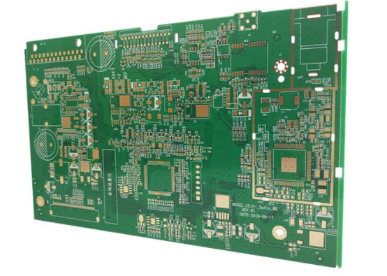
High-frequency board production factory/discussion on the control accuracy of high-frequency PCB characteristic impedance
Circuit board professional production plant: With the rapid development of electronic products, the control of the unique impedance of PCBs has received more stringent requirements.
For example, take the development of high-speed computers as an example to explain the development trend of this demand.
Initially, 800 MHz frequency signal (RMM) was used in the circuit using 800 MHz frequency signal, and the accuracy of the control card (+ 10%) was proposed to ensure that the internal circuit of the host computer and the internal circuit of the switch can achieve higher speeds .
Whether it is RIMM computer products or many electronic products, the circuits on the substrate must match. The accuracy of characteristic impedance control of printed circuit boards used by some customers is not limited to original (+15%) or (10%). Certain precision requirements for impedance control are increased to (+ 8%) or even (+ 5%).
This is a huge challenge for printed circuit manufacturers. This article mainly describes how to meet the strict requirements of customers for impedance accuracy and support counterpart units in the printed circuit manufacturing department.
Impedance control accuracy analysis
In general, the multi-layer card transmission line system can easily reach 60% + 10%, but it is difficult to reach 75% + 5% or even 50 + 5%.
5% error is not common, even in technically demanding applications, but some customers have proposed 5% precision control accuracy, this is an example.
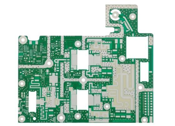
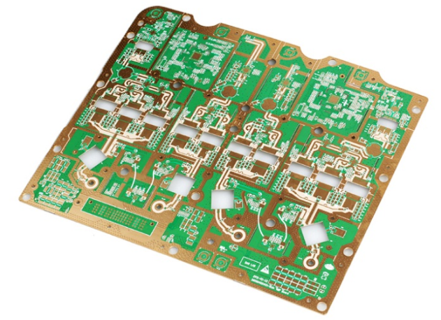
Let’s talk about how to control the characteristic impedance simulation calculation of PCBs. For cards that use impedance control, existing printed circuit manufacturers usually design impedance samples at the appropriate positions of the printed circuit production joints. These impedance samples have the same lamination and impedance. Line structure.

In order to predict the impedance of PCBs, the impedance calculation software must simulate the impedance before designing the impedance sample.
Since 1991, many printed circuit manufacturers have used the United Kingdom Polar test system and computer software.
However, regardless of the strength of the system, the calculation and calculation tools for its calculation and calculation power depend on the use of "ideal" materials.
There is always a certain gap between the simulation results and the actual measured impedance results. Therefore, when the accuracy of the customer's impedance control must be +5%, it is particularly important to use a precise software with accurate calculation accuracy.
There is no accurate forecast.
To this end, we are using the latest development software, the fast Polar SI8000K console, developed by the British Broadcasting Corporation for simulation and prediction.
According to customer requirements:
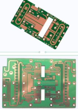
The circuit board can adjust the rolling structure to meet the impedance of 50+5%, but the width of the impedance line cannot be adjusted. Therefore,
The simulation results are as follows: According to the above simulation results, in order to meet the customer's requirement of 50 degrees, the thickness of the dielectric layer should be adjusted from the original second layer to the second layer from 9 to 7 points.
At the same time, in order to meet customer requirements to supplement the thickness of the map, the thickness of the main card needs to be adjusted accordingly. Combined with the internal wiring density,
The structural adjustments are as follows: Control the production of the PCB production process Parallel Expo Since the non-parallel light source is a temporary source, the luminescent light is a kind of scattered light, when it passes through a dry film or another liquid corrosive film The film is exposed to different angles.
The pattern produced by the exposure is different from the pattern of the thin film, and the parallel light will be perpendicular to the dry film or another liquid corroded film.
Therefore, the width of the photosensitive layer exposed on the photosensitive layer is very close to the width on the film, so that a more precise width can be achieved, thereby reducing the influence of such deviation on impedance.
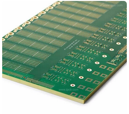
The thin copper foil used for the outer substrate copper foil has developed rapidly due to the rapid development of iron wire, and the copper foil has been greatly developed and fully used. The thickness of the copper foil has increased from one ounce to 1/2 ounce, 1/3 ounce and 1/4 ounce, and even Thinner, such as 1/7 ounce copper foil, developed earlier.
Since the thickness of the copper foil is thin, it is beneficial to the width and integrity of the yarn and the control line, thereby helping to ensure the accuracy of impedance control.
Since the customer's external copper thickness is required to be 1 ounce, we chose 1/3 ounce copper foil to apply pressure to the outer layer of the four-layer board.
After post-plating, the customer's surface copper thickness can reach the thickness of one ounce of copper. This not only responds to customer requirements for copper surface thickness, but also facilitates the control of line width uniformity during the etching process.
Hot-pressed composite copper foil It is heated by electricity and steam. Our company uses a multi-layer vacuum printer produced in Italy and adopts ADRA technology.
The system uses a rolled copper foil to encapsulate the prepreg and laminate layer, and activates the copper foil in the rolling mill to produce heating effects, temperature distribution, and layered temperature distribution. At 177±2°C, the heating speed is high during the hot pressing process, the temperature distribution is uniform, and the fluid uniformity of the resin enables the thickness and plane of the laminate to reach 0.0025 mm, and the interlayer medium can be obtained.