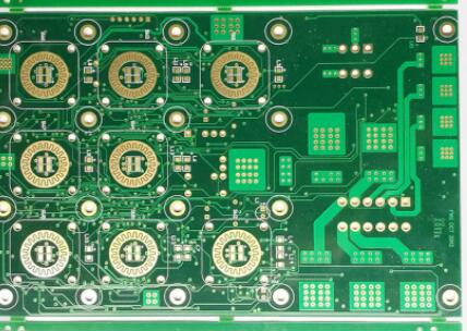
Before designing a multi-layer car lamp circuit board, the designer needs to first determine the circuit board structure used according to the circuit scale, the size of the circuit board and the electromagnetic compatibility (EMC) requirements, that is, the decision to use 4 layers, 6 layers, Or more layers of circuit boards. After determining the number of layers, determine where to place the internal electrical layers and how to distribute different signals on these layers. This is the choice of multilayer PCB stack structure. The laminated structure is an important factor that affects the EMC performance of the car light circuit board, and it is also an important means to suppress electromagnetic interference. The following are design suggestions for your reference.
1. The PCB stacking method is recommended to be the Foil stacking method
2. Minimize the use of PP sheets and CORE models and types in the same stack (each layer of medium does not exceed 3 PP stacks)
3. The thickness of the PP medium between the two layers should not exceed 21MIL (thick PP medium is difficult to process, generally adding a core plate will increase the actual number of layers and increase the processing cost)
4. PCB outer layer (Top, Bottom layer) generally uses 0.5OZ thickness copper foil, and the inner layer generally uses 1OZ thickness copper foil
Note: The copper foil thickness is generally determined according to the size of the current and the thickness of the trace. For example, the power board generally uses 2-3OZ copper foil, and the ordinary signal board generally chooses 1OZ copper foil. If the trace is thinner, 1/3QZ copper may be used. Foil to improve the yield; at the same time, avoid using core boards with inconsistent copper foil thickness on both sides of the inner layer.
5. The distribution of the PCB wiring layer and the plane layer must be symmetrical from the center line of the PCB stack (including the number of layers, the distance from the center line, the copper thickness of the wiring layer and other parameters)

Note: The PCB stacking method needs to adopt a symmetrical design. The symmetrical design refers to the thickness of the insulation layer, the type of prepreg, the thickness of the copper foil, and the pattern distribution type (large copper foil layer, circuit layer) as far as possible relative to the center line of the car light circuit board.
6. The design of line width and medium thickness needs to leave sufficient margin to avoid design problems such as SI caused by insufficient margin
The stack of PCB is composed of power layer, ground layer and signal layer. As the name suggests, the signal layer is the wiring layer of the signal line. The power layer and the ground layer are sometimes collectively referred to as the plane layer.
In a small number of PCB designs, wiring on the power ground plane layer or power and ground network on the wiring layer is used. For this mixed type of layer design, it is collectively called the signal layer.
The figure below is a schematic diagram of a typical stack of 6 layers