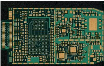
The production of multi-layer PCB in PCB factory must go through a step of pressing. The pressing action includes adding an insulating layer between each layer and bonding each other firmly. If there are vias through several layers. each layer must be processed repeatedly. The wiring on the outer sides of the multilayer board is usually processed after the multilayer board is laminated. There are often some problems in the PCB factory pressing process. let's summarize them together.
White reveals the texture of glass cloth
1. The resin fluidity is too high.
2. the pre-pressure is too high.
3. The timing of adding high pressure is incorrect.
4. The resin content of the bonding sheet is low. the gel time is long. and the fluidity is great.
Foaming
1. The pre-pressure is low.
2. The temperature is too high and the interval between pre-pressure and full pressure is too long.
3. The dynamic viscosity of the resin is high. and the time to add full pressure is too late.
4. The volatile content is too high.
5. The bonding surface is not clean.
6. Poor mobility or insufficient pre-pressure.
7. The board temperature is low.

PCB
There are pits. resin. and wrinkles on the board surface
1. The PCB factory LAY-UP is improperly operated. and the surface of the steel plate is not wiped dry and there are water stains. which causes the copper foil to wrinkle.
2. When pressing the board. the board surface loses pressure. which causes excessive resin loss. lack of glue under the copper foil. and wrinkles on the surface of the copper foil.
The inner layer graphics shift
1. The inner pattern copper foil has low peeling strength or poor temperature resistance or line width is too thin.
2. The pre-pressure is too high and the dynamic viscosity of the resin is small.
3. the press template is not parallel.
Uneven thickness. slippage of the inner layer
1. The total thickness of the forming plate of the same window is different.
2. The accumulated thickness deviation of the printed board in the forming board is large. the parallelism of the hot-pressing template is poor. the laminated board can move freely. and the entire stack is off the center of the hot-pressing template.
Interlayer dislocation
1. The thermal expansion of the inner layer material. the resin flow of the bonding sheet.
2. heat shrinkage during lamination.
3. The thermal expansion coefficients of laminates and templates are quite different.

PCB
Plate curvature. plate warpage
1. asymmetric structure.
2. the curing cycle is insufficient.
3. the cutting direction of the bonding sheet or the inner copper clad laminate is inconsistent.
4. Multilayer boards use plates or bonding sheets from different manufacturers.
5. The multilayer board is not properly handled after post-curing and releasing pressure.
Stratification. heat stratification
1. High humidity or volatile content in the inner layer.
2. High volatile content in the adhesive sheet.
3. inner surface pollution. foreign matter pollution.
4. The surface of the oxide layer is alkaline. there are chlorite residues on the surface.
5. The oxidation is abnormal. and the oxide layer crystal is too long. the pre-treatment has not formed enough surface area.
6. Insufficient passivation.