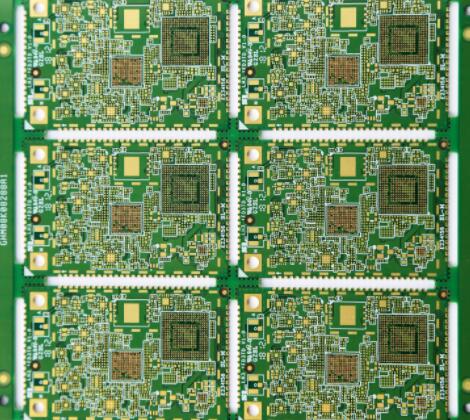
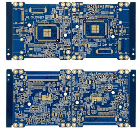
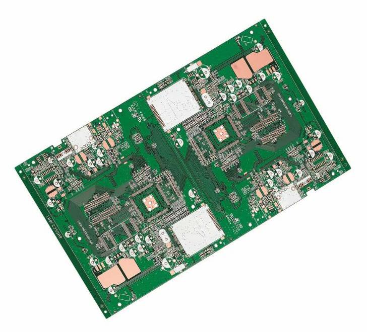
Vias (VIA), the copper foil lines between the conductive patterns in different layers of the circuit board are conducted or connected by this kind of hole, but it is not possible to insert component leads or copper-plated holes of other reinforcing materials. The printed circuit board (PCB) is formed by stacking many layers of copper foil. The copper foil layers cannot communicate with each other because each layer of copper foil is covered with an insulating layer, so they need to rely on vias for signal linking, so there is a Chinese via Title.
The through hole of the smart audio HDI must pass through the plug hole to meet the customer's needs. In changing the traditional aluminum plug hole process, the circuit board surface solder mask and plug hole are completed by white mesh, so that the production is more stable and the quality is better. Reliable and more perfect to use. Vias help circuits to connect and conduct each other. With the rapid development of the electronics industry, higher requirements are placed on the manufacturing process and surface mount technology of printed circuit boards (PCBs).
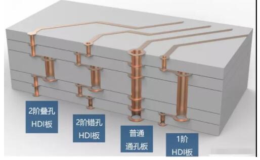
The process of plugging via holes came into being, and at the same time, the following requirements must be met: only copper is required in the hole, and the solder mask can be plugged or not; the hole must have tin-lead and a certain thickness requirement (4um ), avoid the solder mask ink entering the hole, causing tin beads in the hole; the through hole must have a solder mask ink plug hole, opaque, no tin ring and tin beads, and must be flat and other requirements. Blind vias are used to connect the outermost circuit in the printed circuit board(PCB) with the adjacent inner layers with electroplated holes. Since the opposite side cannot be seen, it is called blind pass. In order to increase the space utilization between the board circuit layers, blind holes come in handy. The blind hole is a via hole to the surface of the printed board.
Blind holes are located on the top and bottom surfaces of the smart audio HDI and have a certain depth. They are used to connect the surface line with the inner line below. The depth of the hole generally has a specified ratio (aperture). This production method requires special attention. The drilling depth must be just right. If you don't pay attention, it will cause difficulties in electroplating in the hole. Therefore, few factories will adopt this production method. In fact, it is also possible to drill holes for the circuit layers that need to be connected in advance in the individual circuit layers, and then glue them together, but more precise positioning and alignment devices are required. Buried vias are the connections between any circuit layers inside the printed circuit board (PCB), but they are not connected to the outer layer, that is, they do not have the meaning of via holes extending to the surface of the circuit board.

This production process cannot be achieved by drilling the smart audio HDI after bonding. The drilling operation must be performed on the individual circuit layers. The inner layer is partially bonded and then electroplated, and finally all bonded. Since the operation process is more laborious than the original vias and blind holes, the price is also the most expensive. This manufacturing process is usually only used for high-density circuit boards to increase the space utilization of other circuit layers. In the printed circuit board (PCB) production process, drilling is very important. The simple understanding of drilling is to drill the required vias on the copper clad board, which has the function of providing electrical connections and fixing devices. If the operation is not correct, the process of via holes will be problematic, and the device cannot be fixed on the circuit board, which will affect the use of the circuit board at the slightest, and make the whole board scrapped. Therefore, the drilling process is very important.