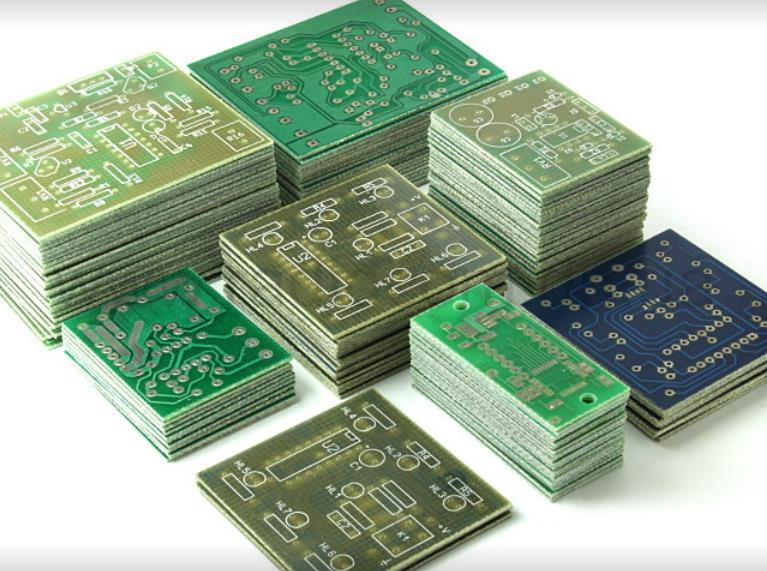
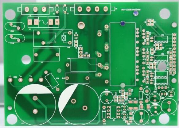
PCB is the heart of every electronic device. Its importance is not only that it allows electrical connections between various components, but also that it carries digital and analog signals, high-frequency data transmission signals, and power lines. With the introduction of 5G technology, the blind and buried via circuit board factory tells you what new needs and requirements PCB needs to meet?
Compared with 4G, the upcoming large-scale deployment of 5G networks will force designers to rethink the PCB design of mobile, IoT, and telecommunications equipment. 5G networks will have the characteristics of high speed, wide bandwidth and low latency, all of which require careful PCB design to support the new high frequency characteristics.
Compared with 4G networks, the fifth-generation mobile technology will provide 10-20 times the transmission rate (up to 1Gbps), up to 1000 times the traffic density and 10 times the number of connections per square kilometer. 5G networks are also designed to provide 1 millisecond latency, which is 10 times faster than the latency provided by 4G networks, and operate over a wider frequency range. The PCB must simultaneously support data rates and frequencies that are much higher than the current data rate, pushing mixed-signal design to the limit. Although the operating frequencies of 4G networks are below the 6GHz threshold (from 600MHz to 5.925GHz), 5G networks will raise the upper frequency limit even higher up to the millimeter wave region (mmWave), with frequency bands centered at 26GHz, 30GHz and 77GHz.
The use of the EHF (very high frequency) frequency band represents one of the most difficult challenges that 5G technology brings to PCB designers. Millimeter waves propagate only through the line of sight, and when they encounter buildings, foliage, or severe weather conditions (such as rain or humidity), they will be strongly attenuated along the way. Therefore, more base stations will be needed to support 5G networks. To support such a large number of frequencies, multiple phased array antennas will be required to support advanced 5G functions, such as beamforming.
Therefore, the blind buried via circuit board tells you that whether it is on a mobile device or a base station, we will have a PCB that integrates a large number of antenna array units (AAU) and extensively uses massive MIMO technology. In Figure 1, we can see a 5G device prototype developed by a leading SoC and telecom modem design company a few years ago. Three active antennas, extremely compact in size, able to manage the frequencies required by the 5G standard, are clearly visible on the top and right side of the PCB.

Figure 1: 5G mobile device prototype (source: Qualcomm)
In addition to frequency, another important challenge is the bandwidth of each channel. Although in the 4G network, the channel bandwidth is set to 20MHz (the IoT device is limited to 200kHz), in the 5G network, its value has been set to 100MHz for frequencies below 6GHz and 400MHz for frequencies above 6GHz. Although there are already modems and radio frequency components that can support these specifications on the market, choosing the most suitable material will be the basis for PCB design. Since the RF front-end will be directly integrated on the PCB, materials with extremely low dielectric transmission loss and extremely high thermal conductivity are required. For frequencies above 6GHz, the materials used to manufacture PCBs must be adapted to special substrates in the millimeter wave frequency band.
The design of 5G application PCB is completely focused on the management of mixed high-speed and high-frequency signals. In addition to the standard rules relating to the design of PCBs with high frequency signals, it is necessary to select the material appropriately in order to prevent power losses and guarantee the integrity of the signal. The EMI that may occur between the part of the analog signal and the part that processes the digital signal, so as to meet the FCC and EMC requirements. The two parameters that guide the selection of materials are the thermal conductivity and the thermal coefficient of the dielectric constant, which describe the change in the dielectric constant (usually in ppm/°C). A substrate with high thermal conductivity is obviously preferable because it can easily dissipate the heat generated by the component. The thermal coefficient of the dielectric constant is an equally important parameter, because the change in the dielectric constant will cause dispersion, which will broaden the digital pulse, change the signal propagation speed, and in some cases will cause signal reflections along the transmission line.
PCB geometry also plays an important role, where geometry means laminate thickness and transmission line characteristics. Regarding the first point, it is necessary to choose a laminate thickness that is usually between 1/4 and 1/8 of the wavelength of the highest operating frequency. If the laminate is too thin, resonance may occur, and it may even propagate waves through the conductor. Regarding the transmission line, it is necessary to decide which type of conductor to use: microstrip, stripline, or grounded coplanar waveguide (GCPW). Microstrip lines may be the most familiar, but they have problems with radiation loss and spurious mode propagation above 30 GHz. Striplines are also an effective solution, but they are difficult to manufacture and therefore more expensive. In addition, micro-holes must be used to connect the ribbon line to the outermost layer. GCPWs are a good choice, but they provide higher conduction losses than microstrip lines and strip lines. After selecting the substrate material, the designer should follow the general rules applicable to high-frequency PCB design: use the shortest possible traces, and check the width and distance between the traces to keep the impedance of all interconnections
constant. The following are some useful suggestions or tips for designing PCBs for 5G applications:
Choose materials with low dielectric constant (Dk): Since Dk loss increases in proportion to frequency, materials with the lowest dielectric constant must be selected;
Use a small amount of solder mask: Most solder masks have a high moisture absorption capacity. If this happens, high losses may occur in the circuit;
Use perfectly smooth copper wire and plan view: The current skin depth is actually inversely proportional to the frequency, so it is very shallow on printed circuit boards with high frequency signals. The irregular copper surface will provide an irregular path for the current and increase the resistance loss;
Signal integrity: High frequency is one of the most difficult challenges faced by IC designers. In order to maximize I/O, high-density interconnect (HDI) requires thinner tracks. This factor can cause signal attenuation, leading to further losses. These losses have an adverse effect on the transmission of radio frequency signals, which may be delayed by a few milliseconds, which in turn causes problems in the signal transmission chain. In the high-frequency domain, signal integrity is almost entirely based on checking impedance. The disadvantage of traditional PCB manufacturing processes, such as the subtractive process, is that it produces tracks with a trapezoidal cross-section (compared to the vertical angle perpendicular to the track, the angle is usually between 25 and 45 degrees). These cross sections change the impedance of the track itself and severely limit 5G applications. However, this problem can be solved by using mSAP (semi-additive manufacturing process) technology, which allows the creation of more precise traces and allows the trace geometry to be defined by photolithography. In Figure 2, we can see the comparison of the two manufacturing processes.

Figure 2: Traditional subtraction and mSAP process
Automatic inspection: PCBs used in high frequency applications need to undergo automatic inspection procedures, including optical (AOI) or through ATE. These procedures allow to greatly improve the quality of the product, highlighting possible errors or inefficiencies in the circuit. Recent advances in the area of automatic PCB inspection and testing have greatly saved time and reduced the costs associated with manual verification and testing. The use of new automatic detection technology will help overcome the challenges brought by 5G, including global impedance control in high-frequency systems. Increasing adoption of automated inspection methods can also achieve consistent performance and high productivity