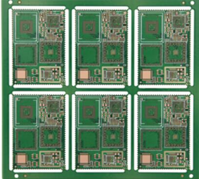
With the development of electronic products in the direction of "light, thin, short, and small", PCBs have also developed to high density and high difficulty. Therefore, a large number of SMT and BGA PCBs appear, and customers require plugging when mounting components; its process The process is long and process control is difficult. So, where is the importance of HDI circuit board plugging process?
1. The HDI circuit board plugging process should meet the following requirements:
1. It is sufficient if there is copper in the via hole, and the solder mask can be plugged or not plugged.
2. There must be tin and lead in the via hole, with a certain thickness requirement (4 microns), and no solder mask ink should enter the hole, causing tin beads to be hidden in the hole.
3. The through hole must have solder mask ink plug hole, opaque, no tin bead, flatness and other requirements.
4. For surface mount boards, especially BGA and IC mounting, the via hole plug holes must be flat, convex and concave plus or minus 1 mil, and there must be no red tin on the edge of the via hole, and tin beads in the via hole, etc. Phenomenon.
2. The plugging process has the following functions:
1. Prevent the HDI circuit board from passing through the component surface through the through hole to cause a short circuit when the HDI circuit board passes through the component surface; if the via hole is placed on the BGA pad, it must be plugged first, and then plated with gold to facilitate the BGA soldering.
2. Avoid flux residue in the vias.
3. Prevent the surface solder paste from flowing into the hole to cause false soldering, which will affect the placement.
4. Prevent the tin bead from popping up during wave soldering, causing short circuit.

3, how does the PCB factory measure the width of the PCB wire
First of all, the PCB factory needs to know whether our purpose is to measure whether the width of the wire obtained after production is consistent with the width of the original circuit design on the customer's circuit pattern.
Secondly, the PCB factory should know what kind of equipment we need for testing. These equipment include a scaled microscope (X50) that can capture 0.001". The microscope can be placed perpendicular to the board surface. Of course, a projection magnifier is the best. .
Finally, the most important step is the entire process of testing. These processes have three main steps.
1) Prepare the test board: We can use the naked eye to select the test area and divide it into 0.500" long straight or curved areas, and then we number them.
2) Test evaluation: Check the width of each 0.500" curve area, and record the results of the test. Defects like some isolated gaps or protrusions are acceptable in principle, but they must be identified and measured.
3) Calculation: The PCB factory takes the width of the middle point between the highest point and the lowest point of each side as the average width of the wires on the parallel sides. We should take the average of the three measurement results in each area for measurement.