The general structure of jumper holes and blind holes is sufficient for high-density circuit boards, but the density of the contacts is not high enough for the structure loading boards that require higher density. Therefore, in the design of higher-density structures, designers will adopt a hole-on-hole design.
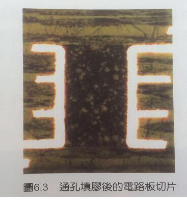
Because ordinary thin dielectric materials do not have enough glue to directly fill the buried holes, the buried through holes must be filled with glue before the surface layer of such a circuit board is made, and the filling process must be smooth Solid, otherwise it is easy to cause the subsequent quality impact due to the filling of too many voids or unevenness. At present, the utilization rate of this type of manufacturing process in electronic package boards is relatively high. In the use of circuit boards, there is a need for thicker buried circuit boards. Of course, it is mainly due to the insufficient filling of the pressure plate glue flow. Figure 6.3 shows the through-hole slice condition of the filled circuit board.

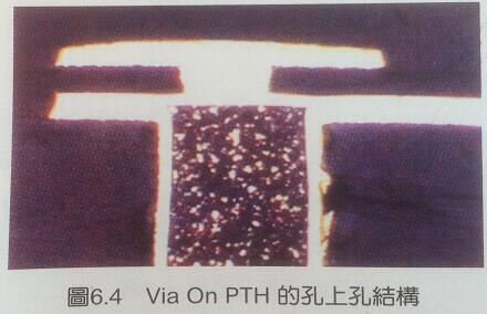
After filling the through holes, the internal circuit must be completed by brushing, removing slag, chemical copper, electroplating and circuit production, and then continue to make the external structure. At this time, in order to increase the density, the cross-connection method adopts the form of holes on the holes. Of course, such a structure has a higher density than indirect connections. Figure 6.4 shows the stacked structure of the holes on the holes.

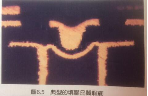
Since the hole filling process may cause residual bubbles to some extent, the residual amount of bubbles will directly affect the quality of the connection. Generally speaking, there is no clear standard for the allowable residual amount of air bubbles. As long as the reliability is not a problem, most of them will not cause injury. However, if the bubbles happen to fall in the area of the orifice, the chances of problems will be relatively increased. As shown in Figure 6.5, it is a typical problem of poor connection caused by filling quality defects.

Because the orifice left air bubbles, a bubble depression was generated after brushing, and a deep hole was left after electroplating. It was not cleaned up during laser processing, so the problem of poor conduction occurred. Therefore, the filling technology will be an important technical problem for the high-density structure loading board, especially for the manufacturers who want to use the hole-on-hole structure.