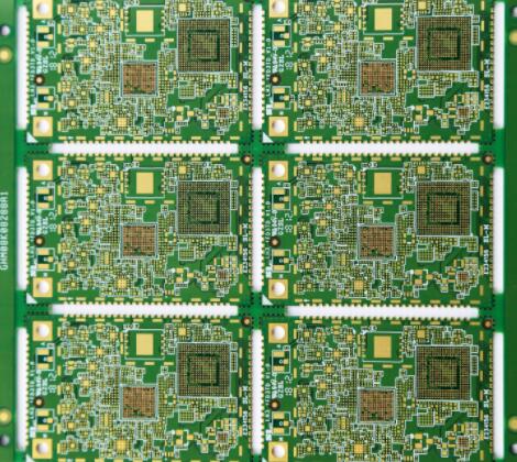
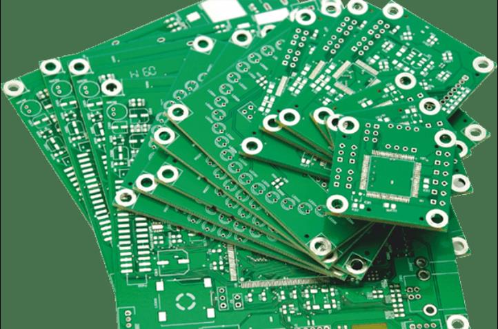
HDI board concept
High-density interconnect printed circuit board(HDI board), HDI: High Density Interconnection.
The American IPC-2315 standard believes that: the minimum designed conductor width and spacing ≤0.10 mm, (mechanical or laser) through aperture ≤0.15 mm, multi-layer printed boards with buried and/or blind holes connected between layers are called HDI board.
HDI board is based on the high density of PCB circuit interconnection. BUM (Build Up Multilayer) refers to the multilayer board made by the build-up process (Build Up Process) production process, also known as build-up board (BU board). The HDI board production mostly uses the build-up process, so it can be said that BUM is also HDI multi-layer board. Also known as MVB (Micro Via Board).
1.2 Features of HDI board
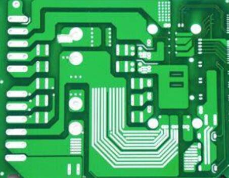
(1) Increase the wiring area and increase the line density;
(2) Reduce the thickness of the insulating medium, reduce the thickness and weight of the entire printed board;
(3) Shorten the wire interconnection length, reduce electrical signal interference and loss;
(4) The thickness-to-diameter ratio of the vias is small, which improves the interconnection reliability;
(5) The structure design of the via hole is convenient, and the design freedom is large, which improves the design efficiency;
(6) Reduce the production cost by reducing the size and number of layers of the printed board.

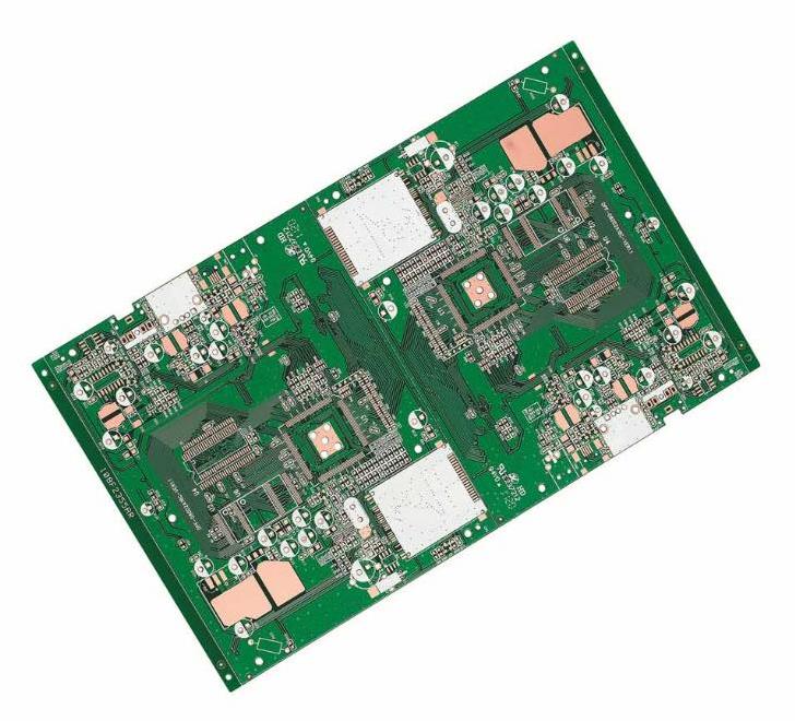
2. What are the uses of HDI circuit boards?
High-density interconnect HDI PCB represents one of the fastest growing segments of the printed circuit board market. Due to the higher circuit density of HDI PCB, thinner lines and spaces, smaller through holes and capture pads, and higher connection pad density can be incorporated in the design. HDI PCBs have blind and buried vias, and usually contain microvias with a diameter of 0.006 or less. So, what are the main applications of HDI PCB circuit boards?
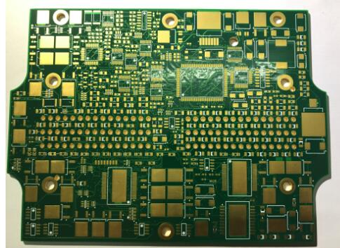
1. The main advantages of HDI PCB The development of HDI PCB technology has brought unprecedented design freedom and flexibility to engineers. More components can be placed on both sides of the original PCB as needed, while allowing smaller components to be placed together.
This means that HDIPCB will eventually lead to faster signal transmission and enhanced signal quality. HDI PCB is widely used to reduce the weight and overall size of products, and to enhance the electrical performance of equipment; it often appears in mobile phones, touch screen devices, notebook computers, digital cameras, and 4G network communications. HDI PCB is also prominent in medical equipment and various electronic aircraft parts.
2. Application of HDI PCB HDI PCB is suitable for various industries. As mentioned above, you will find them in all types of digital devices such as smartphones and tablets, and miniaturization is the key to the effective application of products. You can also find it in cars, airplanes and other vehicles that rely on electronics. One of the most critical areas where high-density PCBs have made great progress is the medical field. Medical equipment often requires small packages with high transmission rates, which only HDI PCB can provide. For example, implants need to be small enough to fit the human body, but any electronic devices involved in the implant absolutely must effectively allow high-speed signal transmission. In addition, other medical equipment, such as emergency room monitors, CT scans, etc. are also available to HDI PCB.