High-density HDI circuit boards are concentrated in 4-layer or 6-layer boards, which are connected to each other according to buried holes, and at least two layers have micro-holes. The main purpose is to better meet the demand for increased I/O with high flip chip density. This technology will quickly be integrated with HDI to complete product miniaturization. High-density substrate HDI is suitable for flip-chip or bonded substrates. The microvia process provides enough space for high-density flip chips. Even HDI products with a 2+2 structure require this technology.
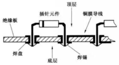
The high-level HDI circuit board is usually a traditional multi-layer board, and the laser perforation is from 1 to 2 layers or 1 to 3 layers. Another feature of it is that micro-holes are processed in the glass fiber reinforced material through the necessary continuous lamination process. The function of this technology is to reserve enough space for components to ensure the required impedance level.
High-level HDI boards are suitable for high-level HDI boards with high I/O counts or fine-pitch components. This product does not require a buried hole process. The purpose of the microvia process is the spacing between high-density devices (such as high I/O devices and ubga). The dielectric material of HDI circuit board products can be copper clad laminate (RCF) or prepreg.

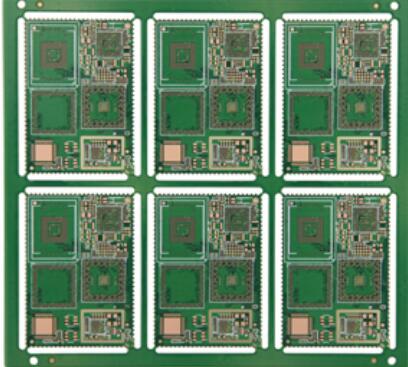
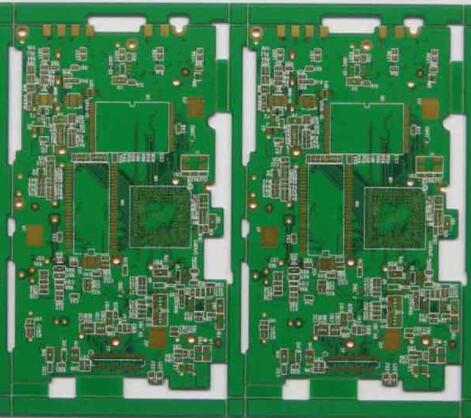
Application of HDI Technology in HDI Industry
one. HDI definition: high-density interconnection lines, the resulting hole diameter is below 0.15mm (6mil) blind hole, the bottom of the blind hole Pad is below 0.25mm (10mil), specially called Microvia microvia or microvia, the line width/spacing is 3mil/mi or finer and narrower.
2. Industrial applications:
The trend of electronic products being lighter, thinner and faster. For small-sized packaged portable electronic devices and the widespread use of high-density interconnections to reduce the demand for component chip products, printed circuit boards are moving towards high-speed technology. Pre-development.
2. The main factors for identifying HDI circuit board technology are:
1) Improve performance, such as data speed and signal integrity.
2) Potential to reduce costs.
3) Reduce weight and energy consumption.
4) Renewal and miniaturization of multilayer board products.