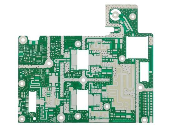
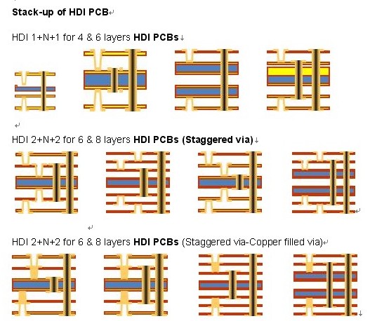
It uses the traditional double-sided board as the core board and is laminated through continuous layering. This kind of circuit board made by continuous layering is also called build-up multilayer (BUM). Compared with traditional circuit boards, HDI circuit boards have the advantages of "light, thin, short, and small". The electrical interconnection between its board layers is achieved through conductive through-holes, buried vias and blind vias. As shown in the figure, its structure is different from ordinary multi-layer circuit boards, and a large number of micro-buried blinds are used in HDI boards. hole.
Traditional multi-layer circuit boards have only through holes and no tiny buried blind holes. The electrical interconnection of this circuit board is realized through through-hole connections. Therefore, high-level numbers are required to meet the design needs. The HDI board uses a micro-buried blind hole design, which can meet the design needs with fewer layers, so it is lighter and thinner. The high density of HDI boards lies in their five major design features compared to traditional printed circuit boards:
1) The board contains blind holes and other micro-guide holes design;
2) The pore diameter is below 152.4μm, and the orifice is below 254μm;
3) The density of welded joints is greater than 50cm/cm2;
4) The wiring density is greater than 46cm/cm2;
5) The width and distance of the circuit should not exceed 76.2μm.

The high density of HDI boards is mainly reflected in three main aspects: holes, lines, and interlayer thickness:
1. Miniaturization of vias. It is mainly manifested in the high requirements of micropore pore-forming technology with a pore diameter of less than 150μm, as well as cost, production efficiency and pore position accuracy control.
2. The refinement of line width and line spacing. It is mainly manifested in the increasingly stringent requirements for wire defects and wire surface roughness.
3. The thickness of the medium is reduced. It is mainly manifested in the trend of interlayer dielectric thickness to 80μm and below, and the requirements for thickness uniformity are becoming more and more stringent, especially for high-density boards and packaging substrates with characteristic impedance control.
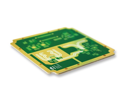
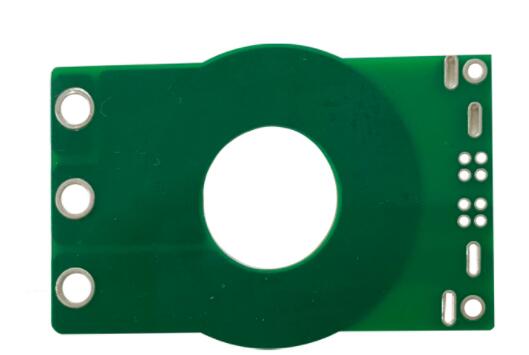
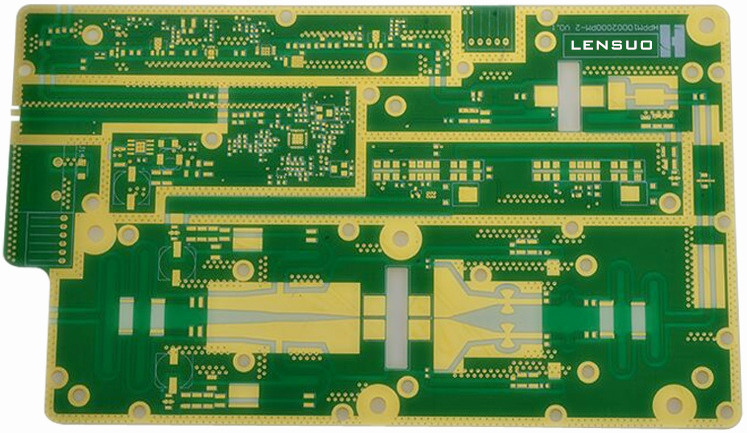
The HDI blind buried via PCB of the original circuit board factory is made like this
With the development of science and technology, the functions of electronic equipment are becoming more and more complex, and higher requirements are put forward on the performance of circuit boards. This has also prompted the emergence of HDI. Gradually, more and more circuit board manufacturers are turning to HDI. develop. The way to increase PCB density is to reduce the number of through holes, and to set blind holes and buried holes.
So what is a blind hole? Today, I will talk to the editor of the PCB board factory to understand what a blind hole is and why the blind hole is so attractive. Blind holes are relative to through holes, and through holes refer to holes drilled through each layer. But blind holes are non-drilled through holes. Blind vias are subdivided into two types, blind vias and buried vias, and the outer layer of the buried vias is invisible. In the production process, blind holes are drilled before pressing, but through holes are drilled after pressing.
When making blind holes, you need to select a through hole first. For each blind hole drilling belt, you need to select a hole and mark the coordinates of its corresponding hole. When making blind holes, you need to pay attention to which drill belt corresponds to which layers. The unit sub-hole diagram and drill tip table need to be marked, and the names of the front and back must be consistent. The icons that cannot appear sub-holes are marked with 1st and 2nd, but the previous label is abc. It is important to note that when the laser hole and the inner buried hole are combined, the two holes are at the same position.
When the circuit board factory produces pnl board edge process holes, the inner layer of the ordinary multilayer board is not drilled. Rivets gh, aoigh, etgh are all etched beer. The outer layer of ghccd needs to be drawn out of copper. After the x-ray machine is directly printed, it is necessary to pay attention to the minimum length of 11 inches.
All tooling holes of the HDI blind hole plate are out of the hole. You need to pay attention to the rivet gh, and it needs to be out to avoid misalignment. The edge of the pnl board needs to be drilled, so that it is convenient to distinguish each board. Film modification needs to indicate the positive and negative film. Generally, the thickness of the board is greater than 8mil, and the process is positive without copper. However, when the board thickness is less than 8mil without copper and thin board, it is the process of taking the negative film. When the line thickness and the fine gap are large, it is necessary to consider the copper thickness of d/f instead of the bottom copper thickness. Finally, it is necessary to note that the inner independent pad corresponding to the blind hole needs to be retained, and the blind hole cannot be made without a ring hole.